EE PRO for TI-89, 92 Plus
Equations - Solid State Devices
99
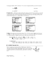
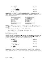
The charging time tch for the CL is defined next. The current in the depletion load I0 is given by the last equation.
tch
CL VL
I
=
⋅
0
Eq. 27.12.5
I
kL VTL
0
2
=
⋅
Eq. 27.12.6
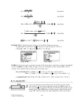
Example 27.12 -
A MOS inverter with a depletion mode transistor as the load has a driver transistor 5_
µ
wide and
1_
µ
long while the load is a depletion mode device with a 0 bias threshold of -4_V, 3_
µ
long and 3_
µ
wide. Given an
electron mobility of 500_cm^2/(V*s) and a depletion threshold of -4_V; for the load device, compute VOH and VTL
when the output voltage is 2.5_V. Assume VOL to be .4_V and .5 for
γ
.
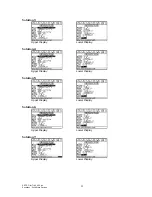
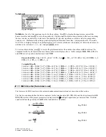
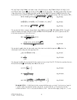
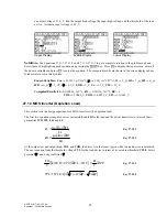
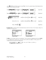
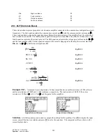
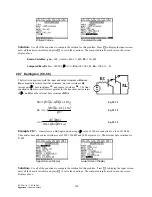
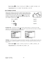
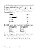
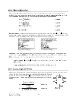
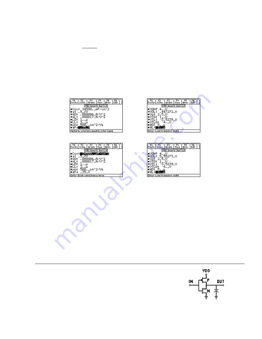
Solution 1: Upper Display
Solution 1: Lower Display
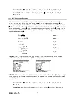
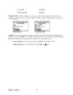
Solution 2: Upper Display
Solution 2: Lower Display
Solution -
The problem can be solved when equations 27.12.1 - 27.12.4 are selected. Highlight each of these and
press
¸
. Press
„
to display the input screen, enter all the known variables and press
„
to solve the equations.
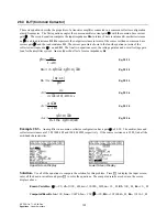
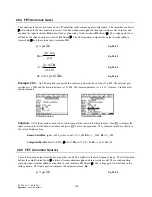
Two complete solutions are computed for this case and are shown in the screen displays above.
-PQYP8CTKCDNGU%QZ
AR(EO@
γ
A8@
.&
A
µ
..
A
µ
µ
P
AEO@8U
φ
(
A8
81*
A8
8Q
A8
86
A8
86.
A8
9&
A
µ
9.
A
µ
%QORWVGF4GUWNVU
5QNWVKQP
M&
A#8@
M.
A#8@
81.
A8
86.
A8
5QNWVKQP
M&
A#8@
M.
A#8@
81.
A8
86.
A8
27.13 CMOS Transistor Pair
These five equations describe the properties of a CMOS inverter. The first two
equations compute device parameters for n and p channel devices. The second pair
of equations compute input voltages VIH and VIL. The last equation computes Vin
when the n-channel driver is in saturation and the p-channel device is in the linear
region.


