background image

23

CIRCUIT OPERATIONAL DESCRIPTION

MPEG B/D SECTION

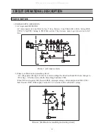
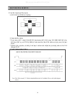
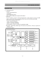
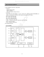
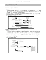
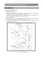
Picture 1.  [ General Block Diagram]

1. Operational Description of MPEG B/D

1) General Operation of B/D
(1) Initial power supply operation 

When the power cord is plugged in, only EVER power is outputted to use minimum power supply such
as u-COM and Flash Memory and MAIN power input is on standby status. 
If Power On Key is inputted, u-COM recognizes it and send Power On (L) signal to POWER, then the
whole power is outputted from POWER and Set is in normal operation.

(2) Function of MPEG B/D

The general Set operation of Key operation and Power supply is controlled by u-COM, and DVD Format
data Decoding and Video, Audio signal separation/output are executed in Loader. 
Here, Video output is in Analog and Audio output is in Digital Data Format to be inputted at Audio DAC.
(See general block diagram below) 

All manuals and user guides at all-guides.com

Summary of Contents for DQD-6100D

Page 1: ...S M No VD6100NET0 Service Manual MODEL DQD 6100D DQD 2100D DAEWOO ELECTRONICS CO LTD Jun 2002 http svc dwe co kr All manuals and user guides at all guides com a l l g u i d e s c o m...

Page 2: ...SPECIFICATIONS 3 CIRCUIT DIAGRAM 4 CIRCUIT OPERATIONAL DESCRIPTION 13 TROUBLE SHOOTING 26 WAVEFORMS 36 COMPONENTS LOCATION GUIDE ON PCB BOTTOM VIEW 45 DISASSEMBLY 47 ELECTRICAL PARTSLIST 51 1 CONTENT...

Page 3: ...DQD 6100D 2 REAR VIEWS 1 DQD 2100D 2 DQD 6100D 2 EXTERNAL VIEWS EURO AV DIGITAL AUDIO OUT AUDIO OUT 2 CH VIDEO OUT EURO AV DIGITAL AUDIO OUT AUDIO OUT 5 1 CH AUDIO OUT 2 CH VIDEO OUT All manuals and u...

Page 4: ...00 resolution available disc DVD CD VCD CD R CD RW DVD R Audio Dolby Digital Analog 5 1ch output and digital output DTS Digital output Convenience Screen zoom function OK Volume control function OK Sp...

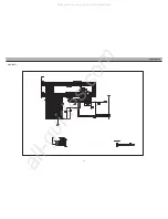
Page 5: ...4 CIRCUIT DIAGRAM POWER SUPPLY SCHEMATIC DIAGRAM DQD 6100 220V All manuals and user guides at all guides com...

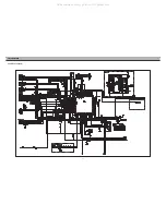
Page 6: ...5 CIRCUIT DIAGRAM VIDEO All manuals and user guides at all guides com a l l g u i d e s c o m...

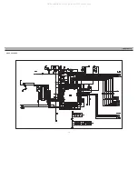
Page 7: ...6 CIRCUIT DIAGRAM AUDIO All manuals and user guides at all guides com...

Page 8: ...7 CIRCUIT DIAGRAM VFD JOG All manuals and user guides at all guides com...

Page 9: ...8 CIRCUIT DIAGRAM ETC All manuals and user guides at all guides com...

Page 10: ...9 CIRCUIT DIAGRAM VCR_INT DVD All manuals and user guides at all guides com...

Page 11: ...10 CIRCUIT DIAGRAM ATAPI DVD All manuals and user guides at all guides com a l l g u i d e s c o m...

Page 12: ...11 CIRCUIT DIAGRAM CPU ZR36703 DVD All manuals and user guides at all guides com...

Page 13: ...12 CIRCUIT DIAGRAM MPEG DECODER All manuals and user guides at all guides com...

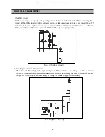
Page 14: ...01 Start Resistor R803 R804 supply Control IC VCC terminal with rectified DC voltage 13 1 POWER SUPPLY OPERATION 1 AC input and EMI FILTER AC inlet consists of Line Filter X Cap Y Cap Varister Line Fi...

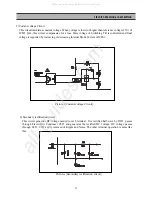
Page 15: ...e is generated between Collector and Emitter it is rectified to D802 smoothed to C807 and consumed to R809 C808 is Speed Up Capacitor 4 Switching and Control Drive Circuit When Base of TR is charged t...

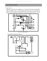
Page 16: ...sing Internal Diode Current of IC801 Picture 5 Costant voltage Circuit 6 Secondary rectification circuit This circuit generates DC voltage needed to each terminal It is rectified half wave by D821 pas...

Page 17: ...o Q822 Base terminal At this time Q824 MOS FET outputs MVCC 5V to Drain terminal and 5V to Source terminal Q823 funcionates in same process and outputs 12M Ever 12V and 12V 2 POWER SUPPLY BLOCK DIAGRA...

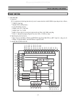
Page 18: ...33 34 35 36 37 38 39 40 41 42 43 44 25 24 23 22 21 20 19 18 17 16 15 14 13 12 11 10 9 8 7 6 5 4 3 2 1 FRONT SECTION 1 VFD DRIVER 1 Overview IC710 implements following functions by serial communication...

Page 19: ...IC500 ZR36705 implements KEY SCAN using VFD DRIVER PT6355 the KEY input DATA go to IC500 by SERIAL Communication then IC500 analyzes and processes the input DATA Implement the operation according to...

Page 20: ...signals by receiving 3 CLOCK System CLOCK Shift CLOCK Left and Right CLOCK and 3 DATA from MPEG DECODER Each 3 DATA associates to 2 CHANNELS DATA1 Main L R CHANNEL DATA2 Surround L R CHANNEL DATA3 Cen...

Page 21: ...DATA from MPEG DECODER and 3 MODE control signal from MICOM and then outputs Analog signal of L R Channel MD Mode Control Data Input MC Mode Control Clock Input ML Mode Control Latch Input BCK Audio...

Page 22: ...C IC300 model outputs 2 Channels to JK301 using only OP AMP IC IC 303 3 Internal Block Diagram 21 CIRCUIT OPERATIONAL DESCRIPTION 4 Hex Inverting Gates IC IC306 1 Overview It consists of 6 independent...

Page 23: ...IC405 at HEX Inverting Gates IC IC306 it outputs Digital signal to Coaxial Jack JK302 2 5 1CH Audio Block Diagram 6 General Audio Operation for 2CH 1 Overview It receives CLOCK and DATA from MPEG DECO...

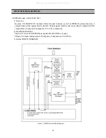
Page 24: ...tus If Power On Key is inputted u COM recognizes it and send Power On L signal to POWER then the whole power is outputted from POWER and Set is in normal operation 2 Function of MPEG B D The general S...

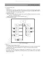
Page 25: ...unction it outputs Analog Video signal directly from IC Output signal could be selected as either Composite S VHS composition or Composite Component Y Cr Cb composition 2 Input Output terminal Input I...

Page 26: ...lated to DVD 2 Input Output terminal Input It receives DVD MPEG Data inputted from Loader Data inputted from Memory and interface Data from IC MPEG Decoder etc Output It outputs Control Data of each I...

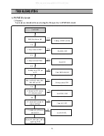
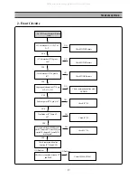
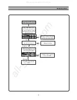
Page 27: ...D825 D826 D827 are OK Exchange POWER code fuse Check L801 L802 Check Q801 Exchange inferior ITEM Check IC801 IC802 NO YES YES YES YES NO NO NO NO 5V obtained at IC802 base and 2 5V obtained at emitter...

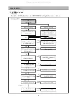
Page 28: ...t Check POWER circuit Check IC 710 Check IC 710 NO YES YES YES YES NO NO NO NO Oscillation at IC710 pin 2 4 YES 1 5VobtainedatR760whenPOWERswitchis pushed 3VobtainedatR761whenOPENswitch ispushed 4Vobt...

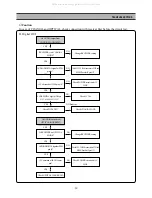
Page 29: ...ding to DVD title Speaker Downmix of SET UP Menu is set on OFF CENTER BACK SUBWOOFER ON ChangeSETUPmenusetting Check signal LINE Check POWER circuit and 5V LINE YES YES YES NO NO NO 5VobtainedatIC350p...

Page 30: ...CEIVER on OPTICAL MODE AUDIODIGITALsignalatP205 pin 1 Change RECEIVER setting Check POWER circuit and 5V LINE YES YES NO NO NO 5V obtained at JK303 center pin Check OPTICAL JACK JK303 CheckFFCCABLEcon...

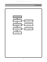
Page 31: ...the VIDEO circuit test check SETUP MENU setting first by remote controller No Component Video output from JK101 TVsettingonSETUPMENUisPALmode YES NO NO NO YES YES VIDEO output of SETUP MENU is set on...

Page 32: ...putofSETUPMENUissetonS Video Is there Video signal from P205 pin 18 19 Check D112 113 114 115 ChangesettingtoPALmode Change setting to S Video CheckFFCCABLEconnectedtoP205 andMPEGDecoderICpin 100 106...

Page 33: ...IC CheckMPEGDecoderIC Check FFC CABLE connected to P481 5 MPEG B D No LOGO display IsPowersupplied YES NO NO NO YES YES Does Oscillation Device oscillate Is Digital Data transmitted from CPU and Flas...

Page 34: ...romCPUand Flash YES NO NO NO YES YES IsDigitalAudioDatatransmittedtoMPEG DecoderICpin 133 IsthereAudiosignalfromP481pin 1 Check Analog B D Check Flash Memory and CPU IC CheckMPEGDecoderIC Check FFC CA...

Page 35: ...deo signal in Q107 Emitter Check D106 and D107 Set it to PAL Check FFC CABLE connecting with P205 and check also IC405 103 pin in MPEG B D Check Q107 No Audio with SCART Jack JK103 Is there Audio sign...

Page 36: ...in Q111 Q112 Base like below each time you press SCART button on remote control Mode Conversion Only when H 3 3V L 0V CheckQ110 Q111andQ112 CheckCABLEconnectingwithP202andcheck alsoIC500 1and 2pininM...

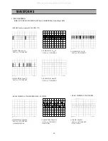
Page 37: ...0 5 2V 3 42VP P 1 73V OFF SET 3 IC500 23PIN 0 1s 2V 3 42VP P 1 73V OFF SET 4 IC500 87PIN 20ms 2V 3 42VP P 1 73V OFF SET 5 IC500 95PIN 10ms 2V 3 42VP P 1 73V OFF SET OS 401 CHRISTAL WAVEFORM 6 OS500 1...

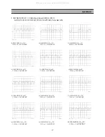
Page 38: ...12 P455 6PIN 0 5 2V 3 19VP P 1 36V OFF SET 13 P455 7PIN 0 5 2V 3 19VP P 1 36V OFF SET 14 P455 8PIN 0 5 2V 3 19VP P 1 36V OFF SET 15 P455 9PIN 0 5 2V 3 19VP P 1 36V OFF SET 16 P455 10PIN 0 5 2V 3 19VP...

Page 39: ...9VP P 1 36V OFF SET 25 P455 23PIN 5ms 1V 2 64VP P 2V OFF SET 26 P455 25PIN 0 5 1V 3 19VP P 1 75V OFF SET 27 P455 27PIN 50ms 0 5V 0 79VP P 3 72V OFF SET 28 P455 31PIN 10ms 1V 3 28VP P 1 6V OFF SET 29 P...

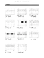
Page 40: ...68PIN MDI 34 P205 3PIN 20ms 2V 3 42VP P 1 71V OFF SET As for instantaneous signal it can t be verified in fact To verify above signal is delayed for the reason of programming IC500 64PIN MC 35 P205 4...

Page 41: ...F SET IC405 105PIN Y R V 44 P205 19PIN 10 1V 1 75V p p 1 3V OFF SET IC405 106PIN C B U 45 P205 20PIN 10 1V 2 3V p p 1 25V OFF SET IC405 103PIN CVBS C 46 P205 23PIN 1ms 2V 4 15V p p 2 07V OFF SET Chang...

Page 42: ...VFD DRIVE IC OUTPUT WAVEFORM 5 AUDIO OUTPUT KDV N TEST DVD VIDEO TITLE2 CHAPTER1 AUDIO DAC OUTPUT WAVEFORM 51 IC710 14PIN 20ms 2V 5 06VP P 2 53V OFF SET 52 IC710 2 4PIN 0 5 0 5V 920mVP P 2 53V OFF SET...

Page 43: ...F SET Noise is almost caught 58 C382 Terminal 0 2ms 50mV 34mVP P 0V OFF SET BNC CABLE use 59 JK300 Front L R Rear L R Center PIN 0 5ms 0 5V 580mVp p 0V OFF SET 60 JK300 WOFER PIN 20ms 10mV 8 7mVP P 0V...

Page 44: ...0 1V 2 3V p p 0V OFF SET CVBS C 65 JK501 blue PIN 10 0 5V 1 72V p p 1 27V OFF SET CVBS G Y 66 JK501 red PIN 10 0 5V 1 72V p p 1 27V OFF SET Y R V 67 JK501 green PIN 10 0 5V 1 95V p p 1 63V OFF SET C B...

Page 45: ...5 0 5V 0V p p 0V OFF SET PC12V in 4 3 AV Mode 74 JK501 8 PIN 0 5 0 5V 0V p p 0V OFF SET DC 6V in 16 9 AV WIDE 71 JK301 3 PIN 0 5 0 2V 292mV p p 0V OFF SET AOL 75 JK103 8 PIN 0 5 0 5V 0V p p 0V OFF SET...

Page 46: ...45 COMPONENTS LOCATION GUIDE ON PCB BOTTOM VIEW All manuals and user guides at all guides com a l l g u i d e s c o m...

Page 47: ...46 JOG COMPONENTS LOCATION GUIDE ON PCB BOTTOM VIEW M P E G All manuals and user guides at all guides com...

Page 48: ...47 DISASSEMBLY All manuals and user guides at all guides com...

Page 49: ...48 DISASSEMBLY All manuals and user guides at all guides com...

Page 50: ...49 DISASSEMBLY All manuals and user guides at all guides com...

Page 51: ...50 DISASSEMBLY All manuals and user guides at all guides com a l l g u i d e s c o m...

Page 52: ...DIODE RGP20D D822 D31DQ09 F DIODE SCHOTTKY 31DQ09 FC5 G701 DHNV10SM21 DIGITRON HNV 10SM21 G701A 97Q2300200 HOLDER DIGITRON ABS H700 10RC356VF4 IC UNIT R RECE1VER ORC0356VF4 38KHZ LOC PATRT CODE PART N...

Page 53: ...C801 1H11A8173S IC PHOTO COUPLER H11A817X 5645D 4P SMD L101 HLM189MD3B L CHIP MULTI 1 8UH 20 2012 L112 HLM189MD3B L CHIP MULTI 1 8UH 20 2012 L113 HLM189MD3B L CHIP MULTI 1 8UH 20 2012 LOC PATRT CODE P...

Page 54: ...ZENER UZ 5 6BSB 5 46 5 70V D101 DZUZ5R6BSB DIODE ZENER UZ 5 6BSB 5 46 5 70V D102 DZUZ5R6BSB DIODE ZENER UZ 5 6BSB 5 46 5 70V D103 DZUZ5R6BSB DIODE ZENER UZ 5 6BSB 5 46 5 70V D106 DZUZ5R6BSB DIODE ZEN...

Page 55: ...R CARBON FILM 1 4 100 OHM J SMALL R102 RD AZ750J R CARBON FILM 1 6 75 OHM J R103 RD 4Z101JS R CARBON FILM 1 4 100 OHM J SMALL R104 RD AZ750J R CARBON FILM 1 6 75 OHM J R106 RD 4Z101JS R CARBON FILM 1...

Page 56: ...ZBA C CHIP CERA 25V Y5V 0 1MF Z 1608 C429 HCFH104ZBA C CHIP CERA 25V Y5V 0 1MF Z 1608 LOC PATRT CODE PART NAME PART DESC C430 HCFH104ZBA C CHIP CERA 25V Y5V 0 1MF Z 1608 C431 HCFH104ZBA C CHIP CERA 25...

Page 57: ...HM 1608 R509 HRFS000 BA R CHIP 1 16 0 OHM 1608 R510 HRFS000 BA R CHIP 1 16 0 OHM 1608 LOC PATRT CODE PART NAME PART DESC R511 HRFS103JBA R CHIP 1 16 10K OHM J 1608 R512 HRFS472JBA R CHIP 1 16 4 7K OHM...

Page 58: ...ZN AZ01A 7173300811 SCREW TAPPTITE TT2 BIN 3X8 MFZN AZ02A 7173300811 SCREW TAPPTITE TT2 BIN 3X8 MFZN D100 97P1R2ZBA0 REMOCON HANDSET AS VR F2ZB M004 97QB248600 DOOR CD AS 2100 M01 97QP322600 PANEL FRO...

Page 59: ...MF K 2012 C824 HCBF683KBA C CHIP CERA X7R 16V 0 068MF K 1608 D801 DS1WBA60 C DIODE BRIDGE S1WBA60 4072 CHIP IC300 1PCM1748KE IC DAC PCM1748KE IC303 1NJM4580MC IC CHIP AMP NJM4580M LOC PATRT CODE PART...

Page 60: ...ZENER UZ 3 0BSB 3 01 3 22V D823 DZGDZP16B DIODE ZENER GDZP16B1 D824 DZEU01Z DIODE EU01Z D825 DZEU01Z DIODE EU01Z D826 DZEU01Z DIODE EU01Z D827 DZZ6R8BM DIODE ZENER UZ 6 8BM AUTO D829 DZUZ13BSB DIODE Z...

Page 61: ...3J R CARBON FILM 1 6 10K OHM J LOC PATRT CODE PART NAME PART DESC R803 RD 4Z394JS R CARBON FILM 1 4 390K OHM J SMALL R804 RD 4Z394JS R CARBON FILM 1 4 390K OHM J SMALL R806 RD 2Z820JS R CARBON FILM 1...

Page 62: ...0K OHM J 1608 R414 HRFS103JBA R CHIP 1 16 10K OHM J 1608 R415 HRFS103JBA R CHIP 1 16 10K OHM J 1608 R416 HRFS103JBA R CHIP 1 16 10K OHM J 1608 LOC PATRT CODE PART NAME PART DESC R417 HRFS330JBA R CHIP...

Page 63: ...S101JBA R CHIP 1 16 100 OHM J 1608 R577 HRFS102JBA R CHIP 1 16 1K OHM J 1608 LOC PATRT CODE PART NAME PART DESC R578 HRFS102JBA R CHIP 1 16 1K OHM J 1608 R579 HRFS102JBA R CHIP 1 16 1K OHM J 1608 R581...

Reviews: