background image

Service manual CP-785AF 

- 7 - 

2 - Safety instruction 


WARNING: 

Only competent service personnel may carry out work involving the testing or repair of 

this equipment. 
 

X-RAY RADIATION PRECAUTION


1.     Excessive high voltage can produce potentially hazardous X-RAY RADIATION. To avoid 
        such hazards, the high voltage must not exceed the specified limit. The nominal value of the high
        voltage of this receiver is 26~28 KV (25” - 29”) at max beam current. The high voltage must not
        under any circumstances, exceed 29.5 KV (25") or 31 KV (29"). 
        Each time a receiver requires servicing, the high voltage should be checked. It is important to
        use an accurate and reliable high voltage meter. 
2. The only source of X-ray Radiation in this TV receiver is the picture tube. For continued X-ray

RADIATION protection, the replacement tube must be exactly the same type tube as specified
in the parts list. 


SAFETY PRECAUTION


1. Potentials of high voltage are present when this receiver is operating. Operation of the receiver 

outside the cabinet or with the back board removed involves a shock hazard from the receiver. 
1)  Servicing should not be attempted by anyone who is not thoroughly familiar with the 

precautions necessary when working on high voltage equipment. 

2) Discharge the high potential of the picture tube before handling the tube. The picture tube is 

highly evacuated and if broken, glass fragments will be violently expelled. 

2. If any Fuse in this TV receiver is blown, replace it with the FUSE specified in the Replacement 

Parts List. 

3. When replacing a high wattage resistor (oxide metal film resistor) in circuit board, keep the resistor 

10 mm away from circuit board. 

4. Keep wires away from high voltage or high temperature components. 
5. This receiver must operate under AC 240 volts, 5O Hz. NEVER connect to DC supply or any 

other power or frequency. 


PRODUCT SAFETY NOTICE


Many electrical and mechanical parts in this equipment have special safety-related characteristics. 
These characteristics are often passed unnoticed by a visual inspection and the X-ray Radiation
protection afforded by them cannot necessarily be obtained by using replacement components rated for 
higher voltage, wattage, etc. Replacement parts which have these special safety characteristics are 
identified in this manual and its supplements, electrical components having such features are identified 
by designated symbol on the parts list. Before replacing any of these components, read the parts list in 
this manual carefully. The use of substitutes replacement parts which do not have the same safety 
characteristics as specified in the parts list may create X-ray Radiation. 


Summary of Contents for DTE-21U6TH

Page 1: ...785AFF0 http svc dwe co kr Apr 2002 DAEWOO ELECTRONICS CO LTD Caution In this Manual some parts can be changed for improving their performance without notice in the parts list So if you need the lates...

Page 2: ...d Processor 18 4 3 TDA894xJ Stereo Audio Amplifier 22 4 4 TDA835xJ Vertical Amplifier 23 4 4 1 TDA8358J 24 4 5 TDA6107Q 25 4 6 24C08 8 Kbit EEPROM 26 4 7 STR F665X 27 5 Circuit description 29 5 1 Bloc...

Page 3: ...cable channels and hyperband Tuning system frequency synthesiser tuning system Visual screen size 21 51 cm Channel indication On Screen Display Program Selection 100 programmes Aux terminal 21 INPUT1...

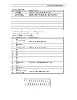
Page 4: ...and S VHS optional SCART 21 pin Euro SCART Input1 S VHS RCA Jack Input1 S VHS not available Pin Signal Description Matching value 1 N C 2 Audio Input Right 0 5 Vrms Impedance 10 k 3 N C 4 Audio Earth...

Page 5: ...5 C06 175 25 C07 182 25 C08 189 25 C09 196 25 C10 209 25 C11 216 75 N01 45 25 N02 55 25 N03 62 25 N08 203 25 N09 210 25 N10 217 25 C21 471 25 C22 479 25 C23 487 25 C24 495 25 C25 503 25 C26 511 25 C27...

Page 6: ...25 C51 687 25 C52 694 25 C53 701 25 C54 708 25 C55 715 25 C56 722 25 C57 729 25 C58 736 25 C59 743 25 C60 750 25 C61 757 25 C62 764 25 C63 771 25 C64 779 25 C65 786 25 C66 793 25 C67 800 25 C68 807 2...

Page 7: ...25 S15 259 25 S16 266 25 S17 273 25 S18 280 25 S19 287 25 S20 294 25 S21 303 25 S22 311 25 S23 319 25 S24 327 25 S25 335 25 S26 343 25 S27 351 25 S28 359 25 S29 367 25 S30 375 25 S31 383 25 S32 391 25...

Page 8: ...age equipment 2 Discharge the high potential of the picture tube before handling the tube The picture tube is highly evacuated and if broken glass fragments will be violently expelled 2 If any Fuse in...

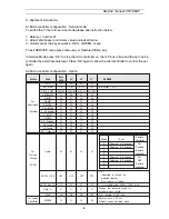
Page 9: ...ection V SHIFT H WIDTH EW Parabola Up Conner Dn Conner EW Trapezium Bare DATA 32 31 31 32 32 32 31 42 25 32 39 13 32 32 32 32 32 32 29 38 31 31 32 32 28 36 34 30 35 19 27 34 37 20 32 32 29 25 38 31 31...

Page 10: ...roller TV in AV mode without video signal Black screen TV preset with WP Red WP Green and WP Blue equal to 32 TV preset with Black R Black G equal to 8 Set TV in NORMAL I mode Adjust screen volume on...

Page 11: ...Corner Dw Corner EW trapez to compensate for geometrical distortion H Parall H Bow H Width EW Parabo la Up Corner Dw Corner EW Trapez 3 3 8 AGC Adjust the antenna signal level at 68 dBmV 2 UHF CH25 S...

Page 12: ...d the bright parts of the screen can be chosen independently l The Text OSD signals are internally supplied from the Controller Teletext decoder l Contrast reduction possibility during mixed mode of O...

Page 13: ...ng CLUT with 4096 colour palette l Globally selectable scan lines per row 9 10 13 16 and character matrix 12x10 12xl3 12x16 VxH l Fringing Shadow selectable from N S E W direction l Fringe colour sele...

Page 14: ...time capture and decoding for WST Teletext in Hardware to enable optimised microprocessor throughput 10 pages stored On Chip lnventory of transmitted Teletext pages stored in the Transmitted Page Tab...

Page 15: ...Service manual CP 785AF A 14...

Page 16: ...ng capability LED 2 11 port 0 6 8mA current sinking capability VSSA 12 analog ground of teletext decoder and digital ground of TV processor SEC PLL 13 SECAM PLL decoupling VP2 14 2nd supply voltage TV...

Page 17: ...t G2IN 47 2nd G input B2IN 48 2nd B input BCLIN 49 beam current limiter input BLKIN 50 black current input R0 51 RED Output G0 52 GREEN Output B0 53 BLUE Output VDDA 54 analog supply of Teletext decod...

Page 18: ...Service manual CP 785AF 17...

Page 19: ...to simultaneously perform digital demodulation and decoding of NICAM coded TV stereo sound as well as demodulation of FM or AM mono TV sound Alternatively two carrier FM systems according to the Germ...

Page 20: ...lly The systems allow two high quality digital sound channels to be added to the already existing FM AM channel The sound coding follows the format of the so called Near Instantaneous Companding Syste...

Page 21: ...no NICAM PAL N A D K 6 5 6 2578125 D K1 6 5 6 7421875 D K2 6 5 5 85 D K NICAM FM Stereo FM Mono NICAM SECAM East N A Architecture of MSP3415D Pin connections and short description Pin No Pin Name Type...

Page 22: ...31 TP Out Test pin 32 NC Not Connected 33 NC Not Connected 34 NC Not Connected 35 VREF1 Reference ground 1 high voltage part 36 SC1_OUT_R Out Scart output 1 right 37 SC1_OUT_L Out Scart output 1 left...

Page 23: ...n all NPN output stage and standby mute logic The TDA8946J comes in a 17 pin DIL power package Features Few external components Fixed gain Standby and mute mode No on off switching plops low standby c...

Page 24: ...and 16 9 picture tubes The circuit provides a DC driven vertical deflection output circuit operating as a highly efficient class G system Due to the full bridge output circuit the deflection coils can...

Page 25: ...current from the diode modulator circuit Features Few external components Highly efficient fully DC coupled vertical output bridge circuit Short rise and fall time of the vertical flyback switch Guard...

Page 26: ...pical bandwidth of 5 5 MHz for an output signal of 60 Vpp High slew rate of 900V ms No external components required Very simple application Single supply voltage of 200V Internal reference voltage of...

Page 27: ...6 SCL Serial clock 7 WC Write control 8 Vcc Supply voltage 4 Vss Ground The memory device is compatible with the I2C memory standard This is a two wire serial interface that uses a bi directionnal da...

Page 28: ...and control IC designed for flyback converter type switch mode power supply applications 4 7 2 Features Small SIP fully isolated molded 5 pins package Many protection functions Pulse by pulse overcurr...

Page 29: ...OFF max 45 55 sec Minimum time for input of quaxi resonant signals 1 5 TTH 2 1 0 sec Minimum off time TOFF min 1 5 sec O C P F B terminal threshold voltage 1 1 5 VTH 1 0 68 0 73 0 78 V O C P F B termi...

Page 30: ...Service manual CP 785AF 29 5 Circuit description 5 1 Block diagram...

Page 31: ...stereo sound processing can be achieved Video switches The video switch has one input for an external CVBS or Y C signal The selected CVBS signal can be supplied to pin 38 the IF video output The sele...

Page 32: ...crystals but has an internal clock generator which is stabilised to the required frequency by using the 12 MHz clock signal from the reference oscillator of the Controller Teletext decoder The Automa...

Page 33: ...ls and nominal settings of the various controls To obtain an accurate biasing of the picture tube the Continuous Cathode Calibration system has been included in these ICs A black level off set can be...

Page 34: ...s tuned using the direct frequency entry or after fine tuning adjustment Therefore it is recommended to tune channel with the TV search function manual or Auto setup or using the direct channel entry...

Page 35: ...ng and cannot be controlled by the software instruction cycle of 1 sec The fast switching pin 16 of SCART 1 is directly connected to the TV processor pin 45 Fast blanking input The display is synchron...

Page 36: ...n Drain High impedance 62 Audio mute Push Pull Push Pull High in stand by mode 5 5 Sound processing Analogue sound IF input section The input pins ANA_IN1 and ANA_IN offer the possibility to connect s...

Page 37: ...ing on the transmitted mode In case of 2 Carrier FM transmission the controlling software read the transmission mode and the signal quality level from the Stereo Detection Register When the set is in...

Page 38: ...E 0 5 V 5 7 Vertical deflection The vertical driver circuit is a bridge configuration The deflection coil is connected between the output amplifiers which are driven in phase opposition The differenti...

Page 39: ...coil EAST WEST Amplifier TDA8358J only The East West amplifier is current driven It can only sink currents of the diode modulator circuit A feedback resistor R397 is connected between the input and o...

Page 40: ...ower supply primary part operations An oscillator generates pulses signals which turn on and off a MOSFET transistor Start up circuit VIN The start up circuit is used to start and stop the operation o...

Page 41: ...ly after the control circuit starts operating VIN starts dropping However as this winding voltage reaches the set value before VIN voltage drops to the shutdown voltage at 11V the control circuit cont...

Page 42: ...omp 1 C1 R1 STR F6653 1 35mA V th 1 V th 2 Oscillating operation O N O N O N O F F O F F O F F M O S F E T s w i t c h i n g O N O F F V D S M O S F E T d r a i n s o u r c e v o l t a g e I D M O S F...

Page 43: ...ermined by C1 and R1 is the OFF time of the MOSFET When C1 voltage falls to around 3 7V the STR F6654 internal oscillator is reversed again and the MOSFET turns ON C1 is quickly charged to around 6 5V...

Page 44: ...ltage is applied to T801 transformer after rectification by D801 D804 diodes Then T801 SMPS transformer starts operating and supplies DC voltage to I823 3 3V regulator This regulator provides 3 3V DC...

Page 45: ...before switching off the microcontroller switches TV set to stand by mode decreasing power pin voltage pin 63 This matter will be explained on paragraph 5 9 2 b Reset pulse circuit 3 3V 3 0V 3 0V 1 2...

Page 46: ...DC supply voltage decreases below 3 V Q510 switches off immediately Q511 starts conducting pulling I501 pin 60 high At the same time it discharges the reset capacitor C501 Discharging this capacitor...

Page 47: ...the power supply circuit diagram is the one shown on the next paragraph power supply circuit diagram during TV set normal run I 8 2 0 5 V R E G U L A T O R I 8 2 3 3 3 V R E G U L A T O R 1 4 5 V C P...

Page 48: ...ltage line includes an IC error amplifier I806 which corrects unexpected DC voltage variations on this line power supply IC delivery during TV set normal run power supply line IC power supply delivery...

Page 49: ...CIRCUIT T801 SM PS TRANS I501 MAIN IC OCP FB D801 D804 GRAETZ BRIDGE 16 D821 I810 controlled rectifier HIGH C841 C840 R713 1 3 1 2 61 64 56 54 7 63 CONDUCTING IR IN com supply voltage KEY IN POWER R88...

Page 50: ...fier gate pin is set to high and I810 is conducting So current flows from pin 16 SMPS transformer to the ground via I804 optocoupler and Q810 and Q811 transistors which are conducting In these conditi...

Page 51: ...RGP30J DIODE RGP30J D820 DRGP30J DIODE RGP30J D860 DRGP30J DIODE RGP30J F801 5FSGB4022L FUSE GLASS TUBE SEMKO TL 4A 250V MF51 HP01 4859102130 JACK EARPHONE YSC 1537 I301 PTB2SW8215 HEAT SINK ASS Y 1TD...

Page 52: ...XE18R432E CRYSTAL QUARTZ HC 49 U 18 43200MHZ 30PPM Z501 5PYXT5R5MB FILTER CERA XT 5 5MB ZZ200 PTMPJ0D454 PCB MAIN RHU AS DTE 21U6TH C305 CEXF1E471V C ELECTRO 25V RSS 470MF 10X16 TP C315 CEXF2C470C C E...

Page 53: ...C351 CCXF1H473Z C CERA 50V F 0 047MF Z TAPPING C370 CMXM2A473J C MYLAR 100V 0 047MF J TP C412 CEXF2C339C C ELECTRO 160V RUS 3 3MF 8X11 5 T C414 CMXM2A104J C MYLAR 100V 0 1MF J TP C418 CCXB1H102K C CER...

Page 54: ...P C610 CEXF1H100V C ELECTRO 50V RSS 10MF 5X11 TP C611 CEXF1H339V C ELECTRO 50V RSS 3 3MF 5X11 TP C612 CEXF1H109V C ELECTRO 50V RSS 1MF 5X11 TP C613 CEXF1H109V C ELECTRO 50V RSS 1MF 5X11 TP C614 CEXF1H...

Page 55: ...104K C MYLAR 250V MEU 0 1MF K F801A 4857415001 CLIP FUSE PFC5000 0702 F801B 4857415001 CLIP FUSE PFC5000 0702 G900 4SG0DX0001 SPARK GAP SSG 102 A1 1 0KV TAP G901 4SG0DX0001 SPARK GAP SSG 102 A1 1 0KV...

Page 56: ...J 5 1A D801 DLT2A05G DIODE LT2A05G TP D802 DLT2A05G DIODE LT2A05G TP D803 DLT2A05G DIODE LT2A05G TP D804 DLT2A05G DIODE LT2A05G TP D805 D1N4937G DIODE 1N4937G TAPPING D806 D1N4937G DIODE 1N4937G TAPPI...

Page 57: ...K OHM J R311 RD AZ102J R CARBON FILM 1 6 1K OHM J R330 RD 2Z121J R CARBON FILM 1 2 120 OHM J R331 RD 2Z151J R CARBON FILM 1 2 150 OHM J R340 RD 4Z473J R CARBON FILM 1 4 47K OHM J R350 RN 4Z1201F R MET...

Page 58: ...R CARBON FILM 1 6 10K OHM J R548 RD AZ472J R CARBON FILM 1 6 4 7K OHM J R549 RD AZ472J R CARBON FILM 1 6 4 7K OHM J R550 RD AZ472J R CARBON FILM 1 6 4 7K OHM J R555 RD AZ103J R CARBON FILM 1 6 10K OHM...

Page 59: ...330 OHM J R829 RD AZ223J R CARBON FILM 1 6 22K OHM J R830 RD AZ332J R CARBON FILM 1 6 3 3K OHM J R840 RD 4Z220J R CARBON FILM 1 4 22 OHM J R841 RD 2Z479J R CARBON FILM 1 2 4 7 OHM J R842 85801065GY WI...

Page 60: ...Service manual CP 785AF 59 7 Exploded view...

Page 61: ...Service manual CP 785AF 60 8 PCB Layout...

Page 62: ...S ervice manual CP 785AF 61 9 Circuit Diagram...

Page 63: ...DAEWOO ELECTRONICS CO LTD 686 AHYEON DONG MAPO GU SEOUL KOREA C P O BOX 8003 SEOUL KOREA TELEX DWELEC K28177 8 CABLE DAEWOOELEC...

Reviews: