background image

51

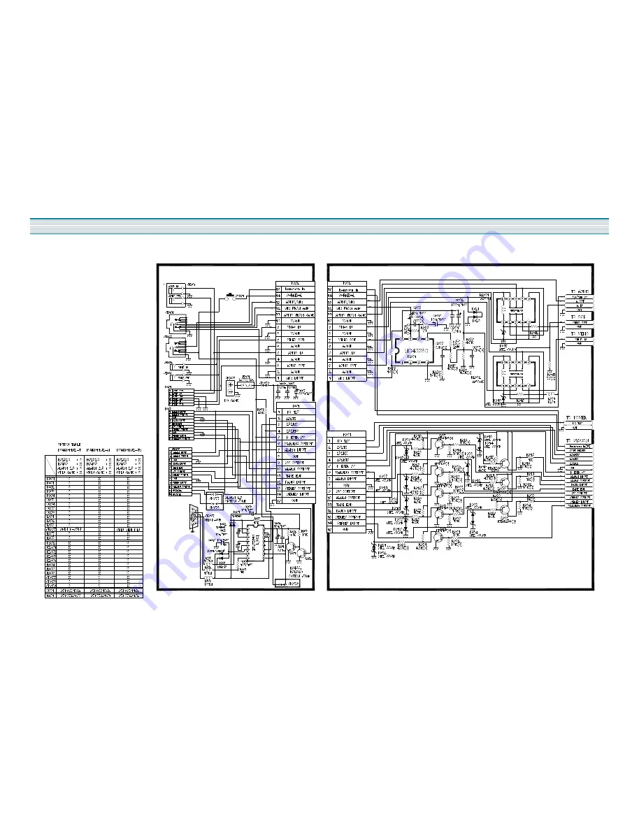
CIRCUIT DIAGRAM

6. TERMINAL CIRCUIT DIAGRAM

All manuals and user guides at all-guides.com

Summary of Contents for DV4K611DZ-T

Page 1: ...T Caution In this Manual some parts can be changed for improving their performance without notice in the parts list So if you need the latest parts information please refer to PPL Parts Price List in...

Page 2: ...RCUIT 29 u COM PORT DESCRIPTION 38 VOLTAGE CHART 41 CIRCUIT DIAGRAM 45 CONNECTION DIAGRAM 45 POWER CIRCUIT DIAGRAM 46 SYSCON CIRCUIT DIAGRAM 47 A V CIRCUIT DIAGRAM 48 OSD CIRCUIT DIAGRAM 49 LOGIC CIRC...

Page 3: ...trengthen between power cord plug prongs and exposed accessible parts of the set RF terminals antenna terminals video and audio input output terminals microphone jack ear phone jacks etc is greater th...

Page 4: ...ure across both terminals of load Z See figure2 and following table Leakage current ratings for selected are as AC Line Voltage Region Load Z Leakage Current i Clearance Distance d d 100V Japan 1k i 1...

Page 5: ...button 5 PAUSE button 6 COUNTER button 7 MENU button 8 STOP button 9 REW button 10 PLAY button 11 FF button 12 CLEAR button 13 SHIFT TRACKING button 14 SHIFT TRACKING button 15 REC PLAY SPEED button...

Page 6: ...S OUT terminal 7 SW OUT terminal 8 TAPE END terminal 9 PANIC IN terminal 10 COM terminal 11 ALARM OUT terminal 12 ALARM IN terminal 13 VIDEO OUT jack 14 VIDEO IN jack 15 AUDIO IN jack 16 AUDIO OUT jac...

Page 7: ...PIN the CH2 to TJ396 video out with CH1 triggering 3 Adjust R595 for the positive trigger until 6 5 0 5H cycle before the vertical SYNC pulse Adjustment Part Checking Point Measuring Equipment Mode T...

Page 8: ...Super Clear Picture Over 300 Lines Horizontal Resolution B W Over 250 Lines Horizontal Resolution Color Various Emergency Record Mode DLC Coating Drum for Long Time Record Various Record Search Alarm...

Page 9: ...B minimum VHS LP 40dB minimum VHS Audio Frequency Range SP 0 3 6dB 100Hz 10KHz VHS LP 0 3 6dB 100Hz 5KHz VHS Distortion SP 4 maximum VHS LP 5 maximum VHS WOW Flutter SP 0 3 maximum VHS LP 0 4 maximum...

Page 10: ...0H LP 6H 18H 30H E 240 SP 4H 64H 72H 128H 160H 224H 320H 480H 640H 960H 1280H LP 8H 24H 40H PLAY MODE E 180 SP 3H 48H 72H 96H 120H 168H 240H 360H 480H 720H 960H LP 6H 18H 30H E 240 SP 4H 64H 72H 128H...

Page 11: ...CAPSTAN SPEED CTL IC501 M37775M5H u COM PROCESSOR Start end SENSOR REEL SENSOR LOADING CAM DRIVE CTL AMP VIDEO BLOCK AUDIO BLOCK TERMINAL BLOCK BACK UP BATT Vcc OSC RESET DV4K611DZ T SERVO SYSCON BLO...

Page 12: ...motor FG numbers DRUM HEAD ON OFF controlled by HEAD AMP SW REC mute signal L R L R L R L R L R L R L 16 65ms 18H EP RECORDING 20FIELD SEC 3H 6H 50FIELD SEC L R L R L 33 3ms 18H 16 7FIELD SEC Recordin...

Page 13: ...m Recording u Trigger Time will be the set time on MENU it will be approximately 2 minutes at least PANIC INPUT This is the first priority REC then operation is similar as Alarm Rec But if Panic Recor...

Page 14: ...ggering video signal with external equipment during recording SERIES OUTPUT When the series recording proceeds after setting the series recording to on this port is used to output the control signal t...

Page 15: ...port is used to receive the control signal to the set which will be recorded continuously after pre recording set WARNING OUTPUT This port is used to inform emergency status of Time Lapse VCR Set to o...

Page 16: ...dicates the signal flow Operating System for installation of SECUNET SW 32Mbytes memory is needed in minimum PC OS System Windows 95 Windows 98 Windows 98 SE Windows ME Windows 2000 Windows NT Pin num...

Page 17: ...tall SECUNET on your computer It is recommended that you exit all other programs before proceed with installation Click Next to continue installation Or click Cancel to cancel installation RS 232C All...

Page 18: ...folder Click Install to begin installation to following folder To install to a different folder Either enter install path Or click Browse and select another folder space needed 3 915bytes RS 232C All...

Page 19: ...18 3 Update your file in the screen above and click Yes 4 To complete installation system must be restarted Click Yes RS 232C All manuals and user guides at all guides com...

Page 20: ...lution If the communication speed of this set isn t equal with that of Personal Computer this set won t be operated properly RS 232C Press RESET button of this set and turn off the timelapse SW Then t...

Page 21: ...us of the Audio 6 Mode of the VCR Displayed mode EJECT STOP FF REC REW PAUSE STILL SLOW CUE1 CUE2 REV1 REV2 STANDBY ERROR1 ERROR2 ERROR3 ERROR4 7 Current time It is the setting time displayed in the V...

Page 22: ...communication speed by pressing down menu of setting in above screen 2 On screen above click SETTING with mouse Then SET will appea Click SET so you can control various communication speed like step3...

Page 23: ...unication speed and comport The communication speed of VCR and Computer is fixed to 9600bps at default value The communication comport of Computer is fixed to COM1 at default value 4 If you click ABOU...

Page 24: ...TIME CLEAR 04 00 02 11 69 CLEAR DRUM USED TIME AUDIO ONOFF 04 00 02 12 68 SELECT AUDIO ON OFF IN LINEAR PLAY REC CHECK 04 00 02 13 67 INDEX FF 04 00 02 14 66 VISS MARK SEARCH FF INDEX REW 04 00 02 15...

Page 25: ...REV1 04BH DREV2 04CH DSTAND 04DH GTZFF 04EH NDXFF 4FH GTZREW 050H NDXREW 051H SHUTREW 052H DPLAY 053H TRCREC 054H OTREC 055H DSTPAUS 056H AUTREW 057H SRCHCUE 058H DSTBEJC 059H DSTP5MIN 05AH NDXPLY 05B...

Page 26: ...SOR NG 0 X X X 1 X X X SP 1 LP EP 0 0 X X 1 X X X X REC INHIBIT 0 X 1 X X X X X END SENSOR 0 1 X X X X X X START SENSOR D7 D6 D5 D4 D3 D2 D1 D0 BIT DESCRIPTION 0 X X X X X X 1 PWRON 0 X X X X X 1 X RE...

Page 27: ...M 3 7 VR TIME STATUS 3 7 1 DATA FORMAT 06H 46H hour minute second day CHECK SUM 3 7 2 VR TIME DATA If the value of DATA is 7FH it means that DATA isn t set The day D7 D6 D5 D4 D3 D2 D1 D0 Status Descr...

Page 28: ...rly Use the isolated transformer and connect GND to the primary GND however it is not necessary to isolate the oscilloscope when check the secondary circuit A CHECKING THE PRIMARY CIRCUIT No output Vo...

Page 29: ...FLOW CHART B CHECKING THE SECONDARY CIRCUIT Check each output voltage Check M801 Check any diode which causes no power Check any COIL or capacitor which causes no power END All manuals and user guides...

Page 30: ...Manual TRK adjust Noise appears although change cassette tape YES Is CTL pulse output at pin 25 of IC501 Playback picture is not good YES NO Check IC501 The voltage of pin 89 of IC501 not changing Che...

Page 31: ...the screen at the bottom Change Drum Ass y Is Enve waveform supplied to pin 4 of P T501 Check connector and Head dust NO NO YES Check pattern Check video circuit Check the PG Adjustment Is SW pulse ap...

Page 32: ...Auto stop during playback NO Is reel pulse applied to pin 5 and 6 of IC501 Check reel sensor NO YES Is D FG applied to pin 24 of IC501 YES Check IC501 Check connector and D FG circuits All manuals an...

Page 33: ...ading stops NO NO Is motor 12V supplied from IC 504 pin 7 8 Check circuit adjacent EVER 12 4V Check power module NO YES YES Is 5 2V supplied from POWER CIRCUIT Check D814 Check connector and motor All...

Page 34: ...stops NO YES Is motor 12V supplied Check power Module NO Is the input of pin 6 of P501 2 7V 3 7V Check circuit of R600 R517 R520 C509 C511 YES NO Is pin 4 of P501 2 5V Check R525 R526 YES NO Does pin...

Page 35: ...of IC501 Check C sync of video IC and pattern Check motor YES Emergency mode when plugging power cord NO YES Is ever 5V applied Check power Module NO Does X501 crystal oscillate Check IC501 and X501 Y...

Page 36: ...S YES YES NO Is motor 12V supplied Check power Module NO NO CAM DATA is changed when CST IN Check connector Check IC501 Check Deck part Is 5V supplied at pin 31 of IC501 Check pattern and R572 All man...

Page 37: ...ES YES YES When mains is unplugged is 3 6V at pin 26 pin 81 of IC501 Check C548 C523 C547 C524 NO Is sine signal applied to pin 42 and 43 of IC501 Check X502 NO Is 5V at pin 37 of IC501 Check reset ci...

Page 38: ...s memory b 800 600 resolution c Windows95 Windows98 Windows ME Windows 98 SE Windows 2000 Windows N T B Hardware Troubleshooting TROUBLESHOOTING FLOW CHART NO NO Impossibility of RS232C communication...

Page 39: ...ck 15 I O OUT C ROTARY Color rotary 16 I O OUT H A SW Head Amp switching 17 I O IN ENVE COMP Enve compare 18 I O OUT PB SW REC MUTE Video switching 19 I O OUT Q V SYNC Q V Sync 20 I O OUT SW OUT Field...

Page 40: ...output 59 I O OUT S6 LED Array segment data output 60 I O OUT S5 LED Array segment data output 61 I O OUT S4 LED Array segment data output 62 I O OUT S3 LED Array segment data output 63 I O OUT S2 LE...

Page 41: ...Adjust 89 I O IN PATH ADJUST Tracking adjust A D IN 90 I O IN PG DELAY PG adjust A D IN 91 I O IN KILLER V Burst or not voltage 92 I O IN DC ENVE Video ENVE A D IN 93 CSYNCIN IN C SYNC Composite sync...

Page 42: ...3 0 3 2 7 3 0 3 0 4 0 0 0 0 8 5 8 5 8 REC PB 1 0 0 0 0 2 5 3 5 3 3 5 3 5 3 REC PB REC PB 1 0 0 0 0 6 0 0 0 0 2 0 5 0 5 7 13 6 13 4 3 0 9 0 9 8 13 6 13 4 4 6 2 6 2 9 0 9 0 9 5 0 0 0 0 10 0 5 0 5 REC P...

Page 43: ...1 2 2 7 4 6 4 6 4 0 0 0 0 8 9 3 9 3 REC PB REC PB 1 8 8 8 8 6 0 0 0 0 2 0 0 0 0 7 0 0 0 0 3 0 0 0 0 8 0 0 0 0 4 0 0 0 0 9 0 0 0 0 5 0 0 0 0 10 0 0 0 0 REC PB REC PB 1 8 7 8 7 6 0 0 0 0 2 0 1 0 1 7 0 1...

Page 44: ...4 41 46 0 5 1 47 0 0 48 5 28 5 3 49 0 0 50 0 0 51 0 0 52 0 12 0 12 53 0 0 54 0 0 55 3 81 0 09 56 3 81 3 82 57 2 22 2 25 58 3 69 2 97 59 0 14 0 15 60 0 87 0 17 61 0 87 0 92 62 0 14 0 17 63 0 14 0 17 6...

Page 45: ...1 1 47 47 9 45 9 46 48 2 14 2 14 49 0 87 0 87 50 0 06 0 06 51 1 8 1 8 52 2 61 2 61 53 0 02 0 02 54 2 62 2 62 55 5 02 5 02 56 3 69 3 68 57 3 39 3 39 58 5 01 5 01 59 3 32 3 32 60 3 59 3 59 61 3 39 3 39...

Page 46: ...45 CONNECTION DIAGRAM CIRCUIT DIAGRAM50 All manuals and user guides at all guides com a l l g u i d e s c o m...

Page 47: ...46 CIRCUIT DIAGRAM 1 POWER CIRCUIT DIAGRAM All manuals and user guides at all guides com...

Page 48: ...47 CIRCUIT DIAGRAM 2 SYSCON CIRCUIT DIAGRAM All manuals and user guides at all guides com...

Page 49: ...48 CIRCUIT DIAGRAM 3 A V CIRCUIT DIAGRAM All manuals and user guides at all guides com...

Page 50: ...49 CIRCUIT DIAGRAM 4 OSD CIRCUIT DIAGRAM All manuals and user guides at all guides com...

Page 51: ...50 CIRCUIT DIAGRAM 5 LOGIC CIRCUIT DIAGRAM All manuals and user guides at all guides com a l l g u i d e s c o m...

Page 52: ...51 CIRCUIT DIAGRAM 6 TERMINAL CIRCUIT DIAGRAM All manuals and user guides at all guides com...

Page 53: ...52 COMPONENTS LOCATION GUIDE ON PCB BOTTOM VIEW 1 PCB MAIN All manuals and user guides at all guides com...

Page 54: ...2 PCB LOGIC All manuals and user guides at all guides com...

Page 55: ...54 COMPONENTS LOCATION GUIDE ON PCB BOTTOM VIEW 3 PCB JACK All manuals and user guides at all guides com...

Page 56: ...55 DISASSEMBLY 1 PANEL FRONT ASS Y All manuals and user guides at all guides com a l l g u i d e s c o m...

Page 57: ...56 DISASSEMBLY 2 SET TOTAL ASS Y All manuals and user guides at all guides com...

Page 58: ...57 DISASSEMBLY 3 PACKING ASS Y All manuals and user guides at all guides com...

Page 59: ...97S8103600 MOTOR L C MDH2B70 B1940 5SSF1DKM10 SW CAM MMS00320ZMBO A1901 7274300611 SCREW TAPTITE TT3 RND 3X6 MFZN A2100 97SA311600 IDLER PLATE AS K MECHA A2200 97S3108200 POLYWASHER D2 6XD6 0XT0 5 A23...

Page 60: ...CH 200PF J 1608 C020 HCFH104ZBA C CHIP CERA 25V Y5V 0 1MF Z 1608 C201 HCBK103KBA C CHIP CERA 50V X7R 0 01MF K 1608 C203 HCBK332KBA C CHIP CERA 50V X7R 3300PF K 1608 C204 HCBK122KBA C CHIP CERA 50V X7R...

Page 61: ...1MF Z 1608 C547 HCFH104ZBA C CHIP CERA 25V Y5V 0 1MF Z 1608 C551 HCFH104ZBA C CHIP CERA 25V Y5V 0 1MF Z 1608 C552 HCBK103KBA C CHIP CERA 50V X7R 0 01MF K 1608 z_loc z_parts_code parts_name parts_desc...

Page 62: ...1 16 100 OHM J 1608 z_loc z_parts_code parts_name parts_descr REMARK R358 HRFS101JBA R CHIP 1 16 100 OHM J 1608 R365 HRFS101JBA R CHIP 1 16 100 OHM J 1608 R372 HRFS392JBA R CHIP 1 16 3 9K OHM J 1608 R...

Page 63: ..._parts_code parts_name parts_descr REMARK R911 HRFS102JBA R CHIP 1 16 1K OHM J 1608 R912 HRFS103JBA R CHIP 1 16 10K OHM J 1608 R913 HRFS103JBA R CHIP 1 16 10K OHM J 1608 R914 HRFS103JBA R CHIP 1 16 10...

Page 64: ...405RA 5R6G RADIAL TP L003 5CPX101J2T COIL PEAKING 100UH BRN BRN L004 5CPX101J2T COIL PEAKING 100UH BRN BRN L201 5CPX100J2T COIL PEAKING 10UH BRN BLK z_loc z_parts_code parts_name parts_descr REMARK L2...

Page 65: ...IAL z_loc z_parts_code parts_name parts_descr REMARK L504 5CPZ121K02 COIL PEAKING 120UH K AXIAL 3 5MM L505 5PB13857 COIL BEAD BI3857 AXIAL L508 5PB13857 COIL BEAD BI3857 AXIAL L509 5PB13857 COIL BEAD...

Page 66: ...AWG22 1 0 65 TIN COATING JP012 WIRE COPPER AWG22 1 0 65 TIN COATING 85801065GY WIRE COPPER JP014 85801065GY AWG22 1 0 65 TIN COATING JP015 WIRE COPPER AWG22 1 0 65 TIN COATING 85801065GY WIRE COPPER J...

Page 67: ...65GY AWG22 1 0 65 TIN COATING z_loc z_parts_code parts_descr REMARK JP109 WIRE COPPER AWG22 1 0 65 TIN COATING 85801065GY WIRE COPPER JP111 85801065GY AWG22 1 0 65 TIN COATING JP112 WIRE COPPER AWG22...

Page 68: ...65 TIN COATING 85801065GY WIRE COPPER JP204 85801065GY AWG22 1 0 65 TIN COATING JP205 WIRE COPPER AWG22 1 0 65 TIN COATING 85801065GY WIRE COPPER JP207 85801065GY AWG22 1 0 65 TIN COATING z_loc z_part...

Page 69: ...3 OHM J R702 RD AZ430J R CARBON FILM 1 6 43 OHM J R703 RD AZ430J R CARBON FILM 1 6 43 OHM J R704 RD AZ430J R CARBON FILM 1 6 43 OHM J R705 RD AZ430J R CARBON FILM 1 6 43 OHM J z_loc z_parts_code parts...

Page 70: ...e parts_name parts_descr REMARK JP962 85801065GY WIRE COPPER AWG22 1 0 65 TIN COATING JP963 85801065GY WIRE COPPER AWG22 1 0 65 TIN COATING JP964 85801065GY WIRE COPPER AWG22 1 0 65 TIN COATING JP965...

Page 71: ...All manuals and user guides at all guides com a l l g u i d e s c o m...

Reviews: