37
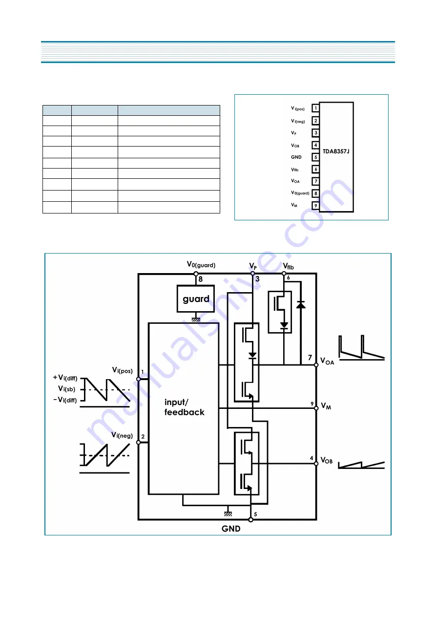
Pinning
Pin
Symbol
Description
1
Vi(pos)
input voltage (positive)
2
Vi(neg)
input voltage (negative)
3
Vp
supply voltage
4
V
OB
output voltage B
5
GND
ground
6
Vflb
flyback supply voltage
7
V
OA
output voltage A
8
V
O(guard)
guard output voltage
9
V
M
input measuring resistor
APPENDIX
IC DESCRIPTION
Summary of Contents for 14C5
Page 3: ...2 CIRCUIT BLOCK DIAGRAM ...
Page 5: ...AUDIO VIDEO ...
Page 6: ...4 Mechanical Exploded View ...
Page 32: ...30 IC DESCRIPTION APPENDIX ...
Page 35: ...33 APPENDIX IC DESCRIPTION ...


