


Service manual SC-150
-31-
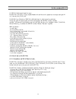
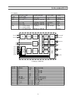
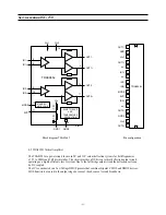
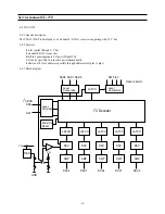
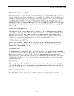
Block diagram TDA8946J
Pin configuration
3
16
Vcc1
Vcc2
IN1-
OUT1-
OUT1-
OUT1+
OUT2-
OUT2+
IN1+
IN1-
IN2-
MODE
SVR
IN2+
n.c.
n.c.
n.c.
GND
GND2
GND1
GND2
Vcc1
Vcc2
OUT1+
OUT2-
OUT2+
IN1+
IN2-
IN2+
MODE
SVR
11
10
STANDBY/
MUTE LOGIC
20
Vcc
15
SHORT CIRCUIT
AND
TEMPERATURE
PROTECTION
20
17
14
4
1
8
6
9
12
TDA8946J
TDA8946J
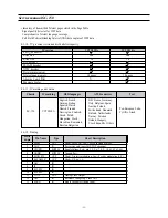
MBK933
1
2
3
4
5
6
7
8
9
10
11
12
13
14
15
16
17
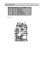
4-5 TDA8358J Vertical Amplifier
The TDA8358J are power circuit for use in 90
o
and 110
o
colour deflection systems for field frequencies
of 25 to 200Hz and 16/9 picture tubes. The circuit provides a DC driven vertical deflection output circuit,
operating as a highly efficient class G system. Due to the full bridge output circuit the deflection coils can
be DC coupled.
The IC is constructed in a Low Voltage DMOS process that combines Bipolar, CMOS and DMOS devices.
MOS transistors are used in the output stage because of the absence of second breakdown.
Summary of Contents for CHASSIS : SC-150 Model : DSC-3220E
Page 35: ...Service manual SC 150 34 Block diagram TDA6107Q...
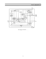
Page 44: ...Service manual SC 150 43 5 Circuit description 5 1 Block diagram...
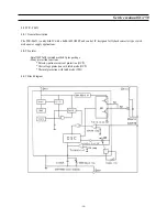
Page 62: ...Service manual SC 150 61 5 9 2 2 STR F6654 oscillating operation...
Page 82: ...Service manual SC 150 81 8 1 PCB MAIN...
Page 83: ...Service manual SC 150 82 8 2 PCB UNION...
Page 84: ...Service manual SC 150 83 9 1 Schematic Diagram MAIN...
Page 85: ...Service manual SC 150 84 9 2 Schematic Diagram UNION...
Page 86: ......


