- 57 -
Service manual WP 895/895F, CP885/885F, CP485F
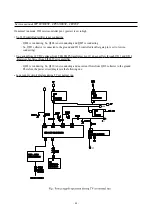
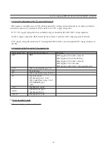
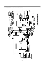
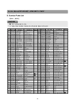
5-7-2 Mode selection
The TDA894xJ has several functional modes, which can be selected by applying the proper DC voltage to pin MODE.
Mute : In this mode the amplifier is DC biased but not operational (no audio output). This allows the input coupling
capacitors to be charged to avoid pop-noise. The device is in mute mode when 2.5 V < V
MODE
< (Vcc-1.5 V).
Operating : In this mode the amplifier is operating normally. The operating mode is activated at V
MODE
< 0.5 V.
5-8 Vertical deflection
The vertical driver circuit is a bridge configuration. The deflection coil is connected between the output amplifiers,
which are driven in phase opposition. The differential input circuit is voltage driven. The input circuit is especially
intended for direct connection to driver circuits which deliver symmetrical current signals, but is also suitable for
asymmetrical currents. The output current of these devices is converted to voltages at the input pins via resistors R350
and R351. The differential input voltage is compared with the output current through the deflection coils measured as
voltage across R398, which provides internal feedback information. The voltage across R398 is proportional to the
output current.
5-8-1 Flyback voltage
The flyback voltage is determined by an additional supply voltage V
flb
. The principle of operation with two supply
voltages (class G) makes it possible to fix the supply voltage Vp optimum for the scan voltage and the second supply
voltage V
flb
optimum for the flyback voltage. Using this method, very high efficiency is achieved. The supply voltage
V
flb
is almost totally available as flyback voltage across the coil, this being possible due to the absence of a coupling
capacitor.
5-8-2 Protection
The output circuit has protection circuits for :
- Too high die temperature
- overvoltage of output stage A
5-8-3 Guard circuit
The guard signal is not used.
5-8-4 Damping resistor
For HF loop stability a damping resistor (R331) is connected across the deflection coil.
5-8-5 EAST-WEST Amplifier (TDA8358J)
The East-West amplifier is current driven. It can only sink currents of the diode modulator circuit. A feedback resistor
R397 is connected between the input and output of this inverting amplifier in order to convert the East-West correction
input into an output voltage.
Summary of Contents for CP-485F
Page 33: ... 32 Service manual WP 895 895F CP885 885F CP485F Block diagram TDA8944J ...
Page 36: ... 35 Service manual WP 895 895F CP885 885F CP485F ...
Page 38: ... 37 Service manual WP 895 895F CP885 885F CP485F Block diagram TDA6107Q ...
Page 43: ... 42 Service manual WP 895 895F CP885 885F CP485F 5 Circuit description 5 1 Block diagram ...
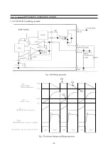
Page 61: ... 60 Service manual WP 895 895F CP885 885F CP485F 5 9 2 2 STR F6654 oscillating operation ...
Page 67: ... 66 Service manual WP 895 895F CP885 885F CP485F ...
Page 87: ...Service Manual WP 895 895F CP885 885F CP485F 86 7 Exploded View 7 1 DWX 28W5 ...
Page 88: ...Service Manual WP 895 895F CP885 885F CP485F 87 7 Exploded View 7 2 DWF 28W8 ...
Page 89: ...Service Manual WP 895 895F CP885 885F CP485F 88 7 Exploded View 7 3 DTF 29U8 ...
Page 90: ...Service Manual WP 895 895F CP885 885F CP485F 89 7 Exploded View 7 4 DTP 28A7 ...
Page 91: ...Service Man ual WP 895 895F CP885 885F CP485F 90 7 Exploded View 7 5 DTP 28B1 ...
Page 92: ...Service Man ual WP 895 895F CP885 885F CP485F 91 7 Exploded View 7 6 DTP 28G7 ...
Page 93: ...Service Manual WP 895 895F CP885 885F CP485F 92 7 Exploded View 7 7 DTP 28G8 ...
Page 94: ...Service Manual WP 895 895F CP885 885F CP485F 7 8 DWF 28W9 93 7 Exploded View ...
Page 95: ... 94 Service Manual WP 895 895F CP885 885F CP 485F 7 9 DTB 21U7 7 Exploded view ...
Page 96: ...SCHEMATIC DIAGRAM WP 895 CP 885 ...
Page 97: ...SCHEMATIC DIAGRAM WP 895F CP 885F ...
Page 98: ...SCHEMATIC DIAGRAM CP 485F ...
Page 99: ......
Page 100: ......
Page 101: ... CP 485F ...

