-42-
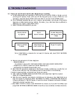
8-1. Facts you must know when trouble diagnosing or repairing.
A. Trouble diagnosing and repairing of set mean find out which PCBs or blocks are not
working and replace them with new PCBs. Repairing the broken PCBs are not
necessary. Keep the broken PCBs and return them to service center or R&D center.
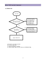
B. This TROUBLE DIAGNOSIS list only contains representative and simple PCB trouble
diagnosis and Module Exchange method. Therefore, if you find Sets that are difficult to
diagnosis or to repair, contact R&D center.
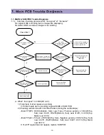
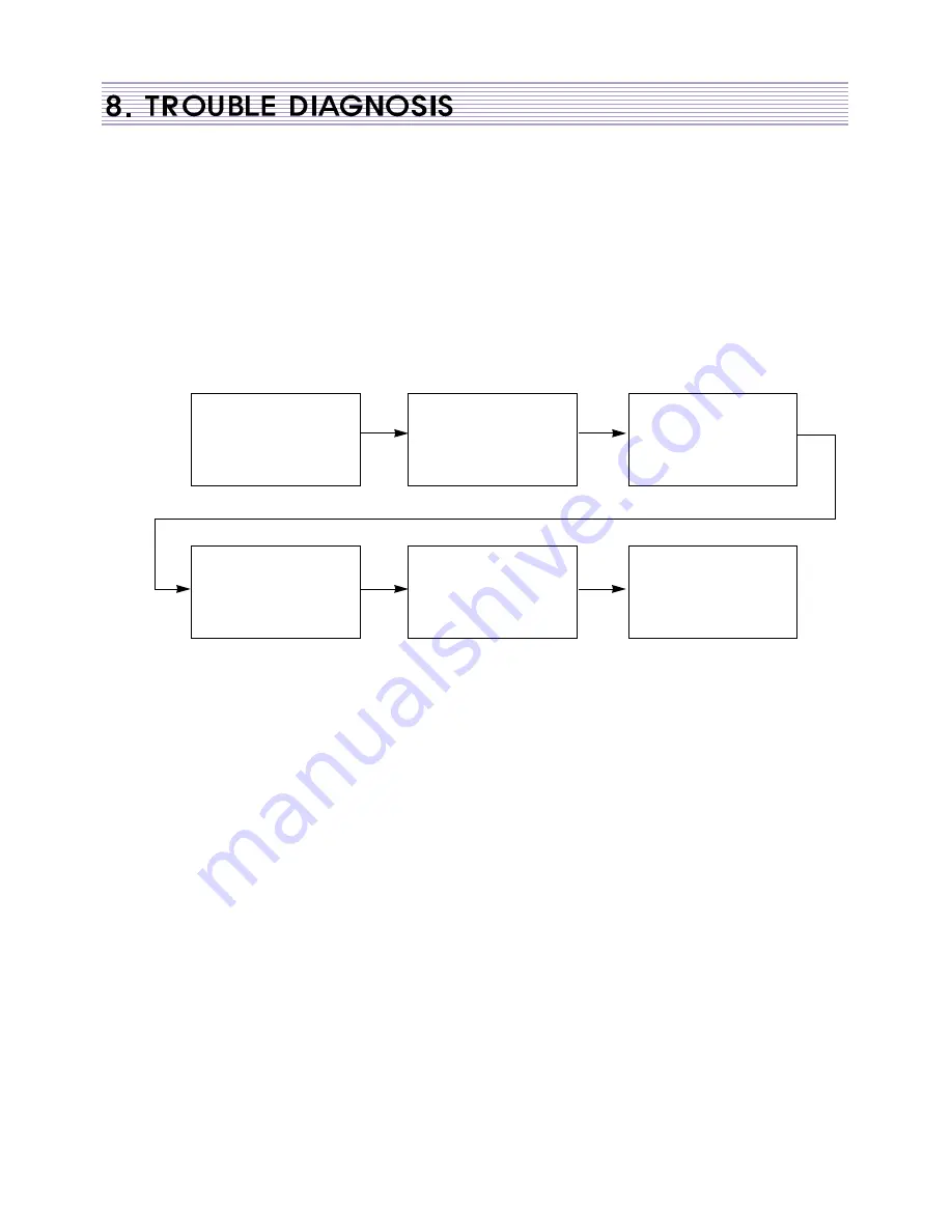
C. Basic TROUBLE DIAGNOSIS process.
D. Required equipments for trouble diagnosis
- Digital Multimeter
User Mode: measure DC VOLTAGE, DIODE VOLTAGE, SHORT/OPEN TEST
- Screwdriver or electric screwdriver, plastic adjusting tool
- Oscilloscope (for detailed examination only)
E. Each BLOCK operations explained in this manual include oscilloscope waveforms, but
these are for reference only and utilizing them to repair PCBs is not necessary.
F. Before replacing PCBs, you MUST turn off the AC switch.
G. After replacing POWER, MAIN and SUB PCB, extra adjustment might be needed.
(Refer to 6. Adjusting Method)
H. After the set is repaired, leave BACK COVER open for followings. Run HEATRUN for at
least 30 minutes by displaying TEST PATTERN (Full White) of SERVICE MODE (Refer
to Service Manual, 5. Service Mode). Check the screen conditions and basic functions.
(Remote Controller operation etc.)
J. After BACK COVER is closed, redo HEATRUN for at least one hour with Full White input
using TEST PATTERN of SERVICE MODE. Check the screen conditions and basic functions.
Note : HEATRUN is conducted for at least 30 minutes with input TEST PATTERN
FULL WHITE
Check problem
Symptoms
Trouble Diagnosis
& Replace broken
PCB
Open
BACK COVER
Adjust new PCB
module
Repair Complete
HEATRUN and
Full Function test
Summary of Contents for DLP-2612
Page 7: ...7 3 2 POWER BLOCK DIAGRAM...
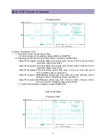
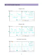
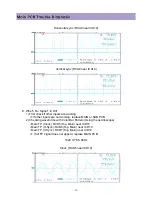
Page 34: ...34 G Signal LCA4 B Signal LCA5 Clock RCA10 near ICA10...
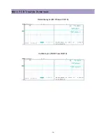
Page 36: ...36 Horizontal sync RCD6 near ICD10 Vertical sync RCD7 near ICD10...
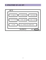
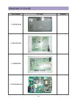
Page 45: ...45 COMPONENT PICTURE REMARK 1 LCD MODULE 2 MAIN BOARD 3 SUB BOARD 4 POWER BOARD...
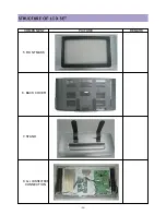
Page 46: ...46 COMPONENT PICTURE REMARK 5 RONT MASK 6 BACK COVER 7 STAND 8 ALL CONNECTROR CONNECTION...
Page 60: ...11 SCHEMATIC DIAGRAM 62...
Page 61: ...SCHEMATIC DIAGRAM 63...
Page 62: ...SCHEMATIC DIAGRAM 64...
Page 63: ...SCHEMATIC DIAGRAM 65...
Page 64: ...SCHEMATIC DIAGRAM 66...
Page 65: ...SCHEMATIC DIAGRAM 67...
Page 66: ...SCHEMATIC DIAGRAM 68...
Page 67: ...SCHEMATIC DIAGRAM 69...
Page 68: ...SCHEMATIC DIAGRAM 70...
Page 69: ...SCHEMATIC DIAGRAM 71...
Page 70: ...SCHEMATIC DIAGRAM 72...
Page 71: ...SCHEMATIC DIAGRAM 73...
Page 72: ...SCHEMATIC DIAGRAM 74...
Page 73: ...SCHEMATIC DIAGRAM 75...
Page 74: ...SCHEMATIC DIAGRAM 76...
Page 75: ...77 10 1 DLP 3212APSB...
Page 76: ...78 10 2 DLP 2612APSB...

