background image

18

CIRCUIT OPERATIONAL DESCRIPTION

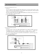
2. Front Part Operational Description

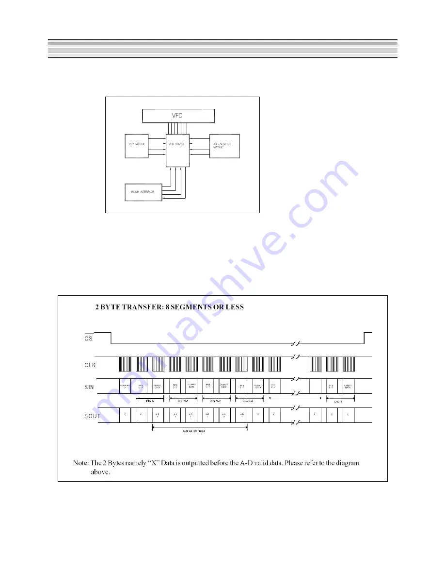
1) KEY SCAN & FLD Driver Interface

2) Operation Description
* If user presses KEY while IC500(ZR36705) implements KEY SCAN using VFD DRIVER(PT6355), the

KEY input DATA go to IC500 by SERIAL Communication, then IC500 analyzes and processes the input
DATA. 

* Implement the operation according to the input command and display the processing status on the VFD

through PT6355

3) Serial Communication Format

Summary of Contents for DQD-2100D

Page 1: ...S M No VD6100NET0 Service Manual MODEL DQD 6100D DQD 2100D DAEWOO ELECTRONICS CO LTD Jun 2002 http svc dwe co kr ...

Page 2: ...T VIEWS 2 2 REAR VIEWS 2 SPECIFICATIONS 3 CIRCUIT DIAGRAM 4 CIRCUIT OPERATIONAL DESCRIPTION 13 TROUBLE SHOOTING 26 WAVEFORMS 36 COMPONENTS LOCATION GUIDE ON PCB BOTTOM VIEW 45 DISASSEMBLY 47 ELECTRICAL PARTSLIST 51 1 CONTENTS ...

Page 3: ...RNT VIEWS 1 DQD 2100D 2 DQD 6100D 2 REAR VIEWS 1 DQD 2100D 2 DQD 6100D 2 EXTERNAL VIEWS EURO AV DIGITAL AUDIO OUT AUDIO OUT 2 CH VIDEO OUT EURO AV DIGITAL AUDIO OUT AUDIO OUT 5 1 CH AUDIO OUT 2 CH VIDEO OUT ...

Page 4: ...izontal frequency over 500 resolution available disc DVD CD VCD CD R CD RW DVD R Audio Dolby Digital Analog 5 1ch output and digital output DTS Digital output Convenience Screen zoom function OK Volume control function OK Special playback function OK MP3 playback function OK Connecting terminal Video terminal Composite terminal 2 unit Component terminal 1 unit S VHS terminal 1 unit Audio terminal ...

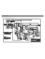
Page 5: ...4 CIRCUIT DIAGRAM POWER SUPPLY SCHEMATIC DIAGRAM DQD 6100 220V ...

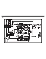
Page 6: ...5 CIRCUIT DIAGRAM VIDEO ...

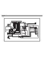
Page 7: ...6 CIRCUIT DIAGRAM AUDIO ...

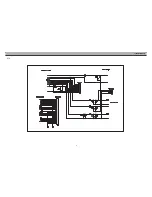
Page 8: ...7 CIRCUIT DIAGRAM VFD JOG ...

Page 9: ...8 CIRCUIT DIAGRAM ETC ...

Page 10: ...9 CIRCUIT DIAGRAM VCR_INT DVD ...

Page 11: ...10 CIRCUIT DIAGRAM ATAPI DVD ...

Page 12: ...11 CIRCUIT DIAGRAM CPU ZR36703 DVD ...

Page 13: ...12 CIRCUIT DIAGRAM MPEG DECODER ...

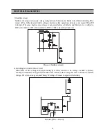
Page 14: ...ent and protects D801 F801 Start Resistor R803 R804 supply Control IC VCC terminal with rectified DC voltage 13 1 POWER SUPPLY OPERATION 1 AC input and EMI FILTER AC inlet consists of Line Filter X Cap Y Cap Varister Line Filter L801 L802 X Cap C803 C888 Y Cap C801 belong to EMI Filter section They decrease noise to get into and out of AC Line CIRCUIT OPERATIONAL DESCRIPTION POWER SECTION Picture ...

Page 15: ...ause high reverse voltage is generated between Collector and Emitter it is rectified to D802 smoothed to C807 and consumed to R809 C808 is Speed Up Capacitor 4 Switching and Control Drive Circuit When Base of TR is charged through starting part TR is turned on So voltage is added to primary winding of transformer and genertaed at Base Drive Because this voltage becomes to Positive Feedback voltage...

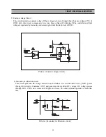
Page 16: ...is regulated by increasing or decreasing Internal Diode Current of IC801 Picture 5 Costant voltage Circuit 6 Secondary rectification circuit This circuit generates DC voltage needed to each terminal It is rectified half wave by D821 passes through Electrolytic Condenser C825 and generates the rectified DC voltage DC voltage passes through L821 C822 and is removed of Ripple and Noise The other term...

Page 17: ...w signal 0V is applied to Q822 Base terminal At this time Q824 MOS FET outputs MVCC 5V to Drain terminal and 5V to Source terminal Q823 funcionates in same process and outputs 12M Ever 12V and 12V 2 POWER SUPPLY BLOCK DIAGRAM NOISE FILTER SUNBBER Switching Primary rectification voltage Control Drive Circuit Costant voltage Control Drive Circuit Starting Part Secondery rectification voltage Picture...

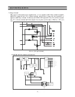
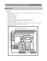
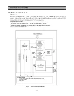
Page 18: ...IT 26 27 28 29 30 31 32 33 34 35 36 37 38 39 40 41 42 43 44 25 24 23 22 21 20 19 18 17 16 15 14 13 12 11 10 9 8 7 6 5 4 3 2 1 FRONT SECTION 1 VFD DRIVER 1 Overview IC710 implements following functions by serial communication with MICOM depending on the software CMOS Technology Internal Pull Low Resistance 4 step Dimming circuitry Output from 8 to 18 Segment Output from 7 to 10 Grid Built in Noise ...

Page 19: ...f user presses KEY while IC500 ZR36705 implements KEY SCAN using VFD DRIVER PT6355 the KEY input DATA go to IC500 by SERIAL Communication then IC500 analyzes and processes the input DATA Implement the operation according to the input command and display the processing status on the VFD through PT6355 3 Serial Communication Format ...

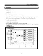
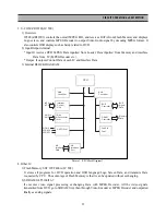
Page 20: ...gital signals to Analog signals by receiving 3 CLOCK System CLOCK Shift CLOCK Left and Right CLOCK and 3 DATA from MPEG DECODER Each 3 DATA associates to 2 CHANNELS DATA1 Main L R CHANNEL DATA2 Surround L R CHANNEL DATA3 Center Woofer CHANNEL During Downmix it receives only DATA1 from MPEG DECODER cf Downmix Sound mixing method using 2 CH when the user doesn t have 6 CH amps or speakers but only h...

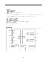
Page 21: ... CONVERTER IC receives 3 CLOCK and 1 DATA from MPEG DECODER and 3 MODE control signal from MICOM and then outputs Analog signal of L R Channel MD Mode Control Data Input MC Mode Control Clock Input ML Mode Control Latch Input BCK Audio Data Bit Clock Input LRCK L Channel and R Channel Audio Data Latch Enable Input SCK System Clock Input DATA Audio Data Digital Input 3 Internal Block Diagram ...

Page 22: ...JK300 cf 2CH Audio DAC IC IC300 model outputs 2 Channels to JK301 using only OP AMP IC IC 303 3 Internal Block Diagram 21 CIRCUIT OPERATIONAL DESCRIPTION 4 Hex Inverting Gates IC IC306 1 Overview It consists of 6 independent gates constructing Logic INVERT function 2 Functions After Noise Filtering Digital audio signal from MPEG DECODER IC405 it outputs the Digital audio signal to Coaxial JK302 3 ...

Page 23: ...ignal from MPEG DECODER IC405 at HEX Inverting Gates IC IC306 it outputs Digital signal to Coaxial Jack JK302 2 5 1CH Audio Block Diagram 6 General Audio Operation for 2CH 1 Overview It receives CLOCK and DATA from MPEG DECODER IC405 and MODE CONTROL signal from MICOM IC500 and transforms Digital signal to Analog signal at AUDIO D A CONVERTER IC300 then amplifies Analog signal IC303 and outputs to...

Page 24: ... input is on standby status If Power On Key is inputted u COM recognizes it and send Power On L signal to POWER then the whole power is outputted from POWER and Set is in normal operation 2 Function of MPEG B D The general Set operation of Key operation and Power supply is controlled by u COM and DVD Format data Decoding and Video Audio signal separation output are executed in Loader Here Video ou...

Page 25: ... well as MPEG Decoding function it outputs Analog Video signal directly from IC Output signal could be selected as either Composite S VHS composition or Composite Component Y Cr Cb composition 2 Input Output terminal Input It receives DVD MPEG Data inputted from MICOM at Loader Output It outputs Analog signal of Composite Component and S VHS etc 3 Internal BLOCK DIAGRAM ...

Page 26: ...ontrols OSD display such as Setup related to DVD 2 Input Output terminal Input It receives DVD MPEG Data inputted from Loader Data inputted from Memory and interface Data from IC MPEG Decoder etc Output It outputs Control Data of each IC and Interface Data 3 Internal BLOCK DIAGRAM 4 Other IC 1 Flash Memory SST 39VF400A IC 502 It stores all programs for DVD operation and OSD language Logo Screen Da...

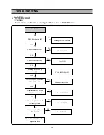
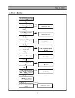
Page 27: ...7 8 D821 D822 D823 D824 D825 D826 D827 are OK Exchange POWER code fuse Check L801 L802 Check Q801 Exchange inferior ITEM Check IC801 IC802 NO YES YES YES YES NO NO NO NO 5V obtained at IC802 base and 2 5V obtained at emitter YES 12VobtainedatQ823drainand 5V obtainedatQ824drain Check D803 D804 D805 3 3VobtainedatQ821 Q822basewhen POWEROFF H YES NO Check Q823 Q824 Q821 Q822 and neighboring ITEM Chec...

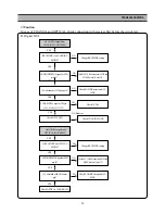
Page 28: ...rcuit Check POWER circuit Check POWER circuit Check IC 710 Check IC 710 NO YES YES YES YES NO NO NO NO Oscillation at IC710 pin 2 4 YES 1 5VobtainedatR760whenPOWERswitchis pushed 3VobtainedatR761whenOPENswitch ispushed 4VobtainedatR762whenPAUSE switchispushed Check communication line with DVD B D Check communication line between IC710 and VFD YES NO Check wire connection between P710 and P900 Chec...

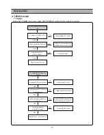
Page 29: ...o Bitstream or PCM according to DVD title Speaker Downmix of SET UP Menu is set on OFF CENTER BACK SUBWOOFER ON ChangeSETUPmenusetting Check signal LINE Check POWER circuit and 5V LINE YES YES YES NO NO NO 5VobtainedatIC350pin 15 YES AUDIOoutputwaveatIC350pin 8 9 10 11 12 13 CheckFFCCABLEconnectedtoP205and MPEGDecoderICpin 130 141 12VobtainedatIC303 304 305pin 8 YES NO AUDIOsignaloutputatIC303 304...

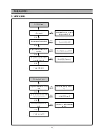
Page 30: ...OPTICAL JACK JK303 Is RECEIVER on OPTICAL MODE AUDIODIGITALsignalatP205 pin 1 Change RECEIVER setting Check POWER circuit and 5V LINE YES YES NO NO NO 5V obtained at JK303 center pin Check OPTICAL JACK JK303 CheckFFCCABLEconnectedtoP205and MPEGDecoderICpin 133 YES YES YES Caution In case of COAXIAL and OPTICAL check connection with receiver first before the circuit test B Digital OUT YES 5V obtain...

Page 31: ...Q101 4 VIDEO circuit Caution Before the VIDEO circuit test check SETUP MENU setting first by remote controller No Component Video output from JK101 TVsettingonSETUPMENUisPALmode YES NO NO NO YES YES VIDEO output of SETUP MENU is set on Component Is there Video signal from P205 pin 17 18 19 Check D116 117 118 119 120 121 ChangesettingtoPALmode Change setting to Component CheckFFCCABLEconnectedtoP20...

Page 32: ...O NO NO YES YES VIDEOoutputofSETUPMENUissetonS Video Is there Video signal from P205 pin 18 19 Check D112 113 114 115 ChangesettingtoPALmode Change setting to S Video CheckFFCCABLEconnectedtoP205 andMPEGDecoderICpin 100 106 NO YES IsthereVideosignalfromQ102 Q103 emitter Check Q102 Q103 ...

Page 33: ...eck Flash Memory and CPU IC CheckMPEGDecoderIC Check FFC CABLE connected to P481 5 MPEG B D No LOGO display IsPowersupplied YES NO NO NO YES YES Does Oscillation Device oscillate Is Digital Data transmitted from CPU and Flash Check SDRAM IC AftercheckingPower_On_L Signalat P505pin 8 checkCPUIC Check OS500 OS401 CheckFlashMemoryandCPUIC NO YES IsDigitalDatatransmittedtoSDRAM fromMPEGDecoderIC Check...

Page 34: ...sDigitalDatatransmittedfromCPUand Flash YES NO NO NO YES YES IsDigitalAudioDatatransmittedtoMPEG DecoderICpin 133 IsthereAudiosignalfromP481pin 1 Check Analog B D Check Flash Memory and CPU IC CheckMPEGDecoderIC Check FFC CABLE connected to P481 ...

Page 35: ... P205 20 pin Is there Video signal in Q107 Emitter Check D106 and D107 Set it to PAL Check FFC CABLE connecting with P205 and check also IC405 103 pin in MPEG B D Check Q107 No Audio with SCART Jack JK103 Is there Audio signal in JK103 1 and 3 pin YES NO Check it with the same method of 2CH Setting of AUDIO circuit 1 Check JK103 and SCART Cable 6 SCART ...

Page 36: ...ontrol NO Is there voltage change in Q111 Q112 Base like below each time you press SCART button on remote control Mode Conversion Only when H 3 3V L 0V Check Q110 Q111 and Q112 CheckCABLEconnectingwithP202andcheck alsoIC500 1and 2pininMPEGB D NO Exchange the bad Item AV AVWide TV Q111Base TV CON H H L Q112Base 16 9 CON L H H Mode Terminal YES Problem Check R150 R151 and check also 12V LINE AV AVWi...

Page 37: ...3V OFF SET 2 IC500 22PIN 0 5 2V 3 42VP P 1 73V OFF SET 3 IC500 23PIN 0 1s 2V 3 42VP P 1 73V OFF SET 4 IC500 87PIN 20ms 2V 3 42VP P 1 73V OFF SET 5 IC500 95PIN 10ms 2V 3 42VP P 1 73V OFF SET OS 401 CHRISTAL WAVEFORM 6 OS500 1PIN 50ns 0 5V 0 18VP P 1 67V OFF SET IC500 92PIN R519 7 OS500 1PIN 50ns 0 5V 1 23VP P 1 7V OFF SET IC500 91PIN 8 OS401 50ns 0 5V 1 09VP P 1 67V OFF SET IC405 119PIN ...

Page 38: ... 3 19VP P 1 36V OFF SET 12 P455 6PIN 0 5 2V 3 19VP P 1 36V OFF SET 13 P455 7PIN 0 5 2V 3 19VP P 1 36V OFF SET 14 P455 8PIN 0 5 2V 3 19VP P 1 36V OFF SET 15 P455 9PIN 0 5 2V 3 19VP P 1 36V OFF SET 16 P455 10PIN 0 5 2V 3 19VP P 1 36V OFF SET 17 P455 11PIN 0 5 2V 3 19VP P 1 36V OFF SET 18 P455 12PIN 0 5 2V 3 19VP P 1 36V OFF SET 19 P455 13PIN 0 5 2V 3 19VP P 1 36V OFF SET 20 P455 14PIN 0 5 2V 3 19VP ...

Page 39: ...24 P455 18PIN 0 5 2V 3 19VP P 1 36V OFF SET 25 P455 23PIN 5ms 1V 2 64VP P 2V OFF SET 26 P455 25PIN 0 5 1V 3 19VP P 1 75V OFF SET 27 P455 27PIN 50ms 0 5V 0 79VP P 3 72V OFF SET 28 P455 31PIN 10ms 1V 3 28VP P 1 6V OFF SET 29 P455 33PIN 1 1V 3 28VP P 1 6V OFF SET 30 P455 35PIN 0 5 1V 3 28VP P 1 6V OFF SET 31 P455 37PIN 0 5 1V 3 28VP P 1 6V OFF SET ...

Page 40: ...son of programming IC500 68PIN MDI 34 P205 3PIN 20ms 2V 3 42VP P 1 71V OFF SET As for instantaneous signal it can t be verified in fact To verify above signal is delayed for the reason of programming IC500 64PIN MC 35 P205 4PIN 10ms 2V 3 42VP P 1 71V OFF SET As for instantaneous signal it can t be verified in fact To verify above signal is delayed for the reason of programming IC500 98PIN ML 36 P2...

Page 41: ...3 P205 18PIN 10 1V 1 75V p p 1 3V OFF SET IC405 105PIN Y R V 44 P205 19PIN 10 1V 1 75V p p 1 3V OFF SET IC405 106PIN C B U 45 P205 20PIN 10 1V 2 3V p p 1 25V OFF SET IC405 103PIN CVBS C 46 P205 23PIN 1ms 2V 4 15V p p 2 07V OFF SET Change only in REMOCON key INPUT IC500 89PIN IRIRQ 47 P205 26PIN 1ms 2V Same with 5 06V p p 2 53V OFF SET 50 IC500 99PIN FPDIN COMPONENT SIGNAL which is OUTPUT in MPEG R...

Page 42: ...T at VFD DRIVE IC 4 VFD VFD DRIVE IC OUTPUT WAVEFORM 5 AUDIO OUTPUT KDV N TEST DVD VIDEO TITLE2 CHAPTER1 AUDIO DAC OUTPUT WAVEFORM 51 IC710 14PIN 20ms 2V 5 06VP P 2 53V OFF SET 52 IC710 2 4PIN 0 5 0 5V 920mVP P 2 53V OFF SET 53 IC710 18PIN 2ms 5V 27 5VP P 13 7V OFF SET 54 IC350 8PIN 0 5ms 0 5V 500mVP P 2 5V OFF SET 10 11 12 13 PIN 55 IC350 9PIN 1 200mV 146mVP P 2 5V OFF SET BNC CABLE L R LS RS C L...

Page 43: ... 200mV 175mVP P 5 89V OFF SET Noise is almost caught 58 C382 Terminal 0 2ms 50mV 34mVP P 0V OFF SET BNC CABLE use 59 JK300 Front L R Rear L R Center PIN 0 5ms 0 5V 580mVp p 0V OFF SET 60 JK300 WOFER PIN 20ms 10mV 8 7mVP P 0V OFF SET BNC CABLE 61 IC306 12PIN 0 5 1V 3 3V p p 1 75V OFF SET 62 JK302 Coaxial Pin 0 5 1V 0 68V p p 0V OFF SET 63 JK303 Optical 0 5 2V 3 28V p p 1 66V OFF SET COAXIAL FINALOU...

Page 44: ...PUT 64 JK301 yellowPIN 10 1V 2 3V p p 0V OFF SET CVBS C 65 JK501 blue PIN 10 0 5V 1 72V p p 1 27V OFF SET CVBS G Y 66 JK501 red PIN 10 0 5V 1 72V p p 1 27V OFF SET Y R V 67 JK501 green PIN 10 0 5V 1 95V p p 1 63V OFF SET C B U 68 JK502 2PIN 10 1V 1 87V p p 1 13V OFF SET Y R V 69 JK502 1PIN 10 1V 1 75V p p 1 35V OFF SET C B U ...

Page 45: ...SET AOR 73 JK103 8PIN 0 5 0 5V 0V p p 0V OFF SET PC12V in 4 3 AV Mode 74 JK501 8 PIN 0 5 0 5V 0V p p 0V OFF SET DC 6V in 16 9 AV WIDE 71 JK301 3 PIN 0 5 0 2V 292mV p p 0V OFF SET AOL 75 JK103 8 PIN 0 5 0 5V 0V p p 0V OFF SET DC 0V in TV Mode CONTROL SIGNAL VIDEO OUTPUT 72 JK103 19 PIN 10 1V 2V p p 0V OFF SET L R 1KHz 1KHz 20dB 20dB ...

Page 46: ...45 COMPONENTS LOCATION GUIDE ON PCB BOTTOM VIEW ...

Page 47: ...46 JOG COMPONENTS LOCATION GUIDE ON PCB BOTTOM VIEW M P E G ...

Page 48: ...47 DISASSEMBLY ...

Page 49: ...48 DISASSEMBLY ...

Page 50: ...49 DISASSEMBLY ...

Page 51: ...50 DISASSEMBLY ...

Page 52: ...GREEN BULK D821 DRGP20D DIODE RGP20D D822 D31DQ09 F DIODE SCHOTTKY 31DQ09 FC5 G701 DHNV10SM21 DIGITRON HNV 10SM21 G701A 97Q2300200 HOLDER DIGITRON ABS H700 10RC356VF4 IC UNIT R RECE1VER ORC0356VF4 38KHZ LOC PATRT CODE PART NAME PART DESC JK102 97Q6316200 JACK DIN DUAE 9619 JK103 97P6318110 SCART JACK DSAM 9871 JK300 97P6318130 JACK PIN DPAM 0219 JK301 97P6318140 JACK PIN DPAM 0220 JK302 97P6318050...

Page 53: ...R PT6355 44LQFP VFD DR IC801 1H11A8173S IC PHOTO COUPLER H11A817X 5645D 4P SMD L101 HLM189MD3B L CHIP MULTI 1 8UH 20 2012 L112 HLM189MD3B L CHIP MULTI 1 8UH 20 2012 L113 HLM189MD3B L CHIP MULTI 1 8UH 20 2012 LOC PATRT CODE PART NAME PART DESC R100 HRFS750JBA R CHIP 1 16 75 OHM J 1608 R112 HRFS750JBA R CHIP 1 16 75 OHM J 1608 R113 HRFS750JBA R CHIP 1 16 75 OHM J 1608 R114 HRFS750JBA R CHIP 1 16 75 ...

Page 54: ...0N D100 DZUZ5R6BSB DIODE ZENER UZ 5 6BSB 5 46 5 70V D101 DZUZ5R6BSB DIODE ZENER UZ 5 6BSB 5 46 5 70V D102 DZUZ5R6BSB DIODE ZENER UZ 5 6BSB 5 46 5 70V D103 DZUZ5R6BSB DIODE ZENER UZ 5 6BSB 5 46 5 70V D106 DZUZ5R6BSB DIODE ZENER UZ 5 6BSB 5 46 5 70V D107 DZUZ5R6BSB DIODE ZENER UZ 5 6BSB 5 46 5 70V D112 DZUZ5R6BSB DIODE ZENER UZ 5 6BSB 5 46 5 70V D113 DZUZ5R6BSB DIODE ZENER UZ 5 6BSB 5 46 5 70V D114 ...

Page 55: ...7 AXIAL R101 RD 4Z101JS R CARBON FILM 1 4 100 OHM J SMALL R102 RD AZ750J R CARBON FILM 1 6 75 OHM J R103 RD 4Z101JS R CARBON FILM 1 4 100 OHM J SMALL R104 RD AZ750J R CARBON FILM 1 6 75 OHM J R106 RD 4Z101JS R CARBON FILM 1 4 100 OHM J SMALL R107 RD AZ750J R CARBON FILM 1 6 75 OHM J R115 RD 4Z101JS R CARBON FILM 1 4 100 OHM J SMALL LOC PATRT CODE PART NAME PART DESC R117 RD 4Z101JS R CARBON FILM 1...

Page 56: ...RA 25V Y5V 0 1MF Z 1608 C428 HCFH104ZBA C CHIP CERA 25V Y5V 0 1MF Z 1608 C429 HCFH104ZBA C CHIP CERA 25V Y5V 0 1MF Z 1608 LOC PATRT CODE PART NAME PART DESC C430 HCFH104ZBA C CHIP CERA 25V Y5V 0 1MF Z 1608 C431 HCFH104ZBA C CHIP CERA 25V Y5V 0 1MF Z 1608 C432 HCFH104ZBA C CHIP CERA 25V Y5V 0 1MF Z 1608 C444 HCQK100JBA C CHIP CERA 50V CH 10PF J 1608 C445 HRFS000 BA R CHIP 1 16 0 OHM 1608 C450 HCQK1...

Page 57: ...FS000 BA R CHIP 1 16 0 OHM 1608 R509 HRFS000 BA R CHIP 1 16 0 OHM 1608 R510 HRFS000 BA R CHIP 1 16 0 OHM 1608 LOC PATRT CODE PART NAME PART DESC R511 HRFS103JBA R CHIP 1 16 10K OHM J 1608 R512 HRFS472JBA R CHIP 1 16 4 7K OHM J 1608 R513 HRFS472JBA R CHIP 1 16 4 7K OHM J 1608 R514 HRFS330JBA R CHIP 1 16 33 OHM J 1608 R515 HRFS330JBA R CHIP 1 16 33 OHM J 1608 R516 HRFS330JBA R CHIP 1 16 33 OHM J 160...

Page 58: ... TAPPTITE TT2 BIN 3X8 MFZN AZ01A 7173300811 SCREW TAPPTITE TT2 BIN 3X8 MFZN AZ02A 7173300811 SCREW TAPPTITE TT2 BIN 3X8 MFZN D100 97P1R2ZBA0 REMOCON HANDSET AS VR F2ZB M004 97QB248600 DOOR CD AS 2100 M01 97QP322600 PANEL FRONT AS DQD 2100 B010 7174300811 SCREW TAPPTITE TT2 RND 3X8 MFZN M01A 7173302011 SCREW TAPTITE TT2 BIN 3X20 MFZN M1000 97Q6009400 DRIVE DVD RL A700 P202A 97P885X150 CONN ASSY 10H...

Page 59: ... CHIP CERA 50V X7R 0 047MF K 2012 C824 HCBF683KBA C CHIP CERA X7R 16V 0 068MF K 1608 D801 DS1WBA60 C DIODE BRIDGE S1WBA60 4072 CHIP IC300 1PCM1748KE IC DAC PCM1748KE IC303 1NJM4580MC IC CHIP AMP NJM4580M LOC PATRT CODE PART NAME PART DESC IC306 1DM74LS04M IC INVERT DM74LS04MX IC710 1PT6355 IC DRIVER PT6355 44LQFP VFD DR IC801 1H11A8173S IC PHOTO COUPLER H11A817X 5645D 4P SMD L101 HLM189MD3B L CHIP...

Page 60: ...M D805 DZUZ3R0BSB DIODE ZENER UZ 3 0BSB 3 01 3 22V D823 DZGDZP16B DIODE ZENER GDZP16B1 D824 DZEU01Z DIODE EU01Z D825 DZEU01Z DIODE EU01Z D826 DZEU01Z DIODE EU01Z D827 DZZ6R8BM DIODE ZENER UZ 6 8BM AUTO D829 DZUZ13BSB DIODE ZENER UZ 13BSB 12 59 13 16V JP001 85801065GY WIRE COPPER AWG22 1 0 65 TIN COATING JP002 85801065GY WIRE COPPER AWG22 1 0 65 TIN COATING JP003 85801065GY WIRE COPPER AWG22 1 0 65...

Page 61: ...BON FILM 1 6 5 6K OHM J R774 RD AZ103J R CARBON FILM 1 6 10K OHM J LOC PATRT CODE PART NAME PART DESC R803 RD 4Z394JS R CARBON FILM 1 4 390K OHM J SMALL R804 RD 4Z394JS R CARBON FILM 1 4 390K OHM J SMALL R806 RD 2Z820JS R CARBON FILM 1 2 82 OHM J SMALL R808 RD 2Z820JS R CARBON FILM 1 2 82 OHM J SMALL R811 RC 2Z565KP R CARBON COMP 1 2 5 6M OHM K R822 RD AZ132G R CARBON FILM 1 6 1 3K OHM G R823 RD A...

Page 62: ...HRFS103JBA R CHIP 1 16 10K OHM J 1608 R414 HRFS103JBA R CHIP 1 16 10K OHM J 1608 R415 HRFS103JBA R CHIP 1 16 10K OHM J 1608 R416 HRFS103JBA R CHIP 1 16 10K OHM J 1608 LOC PATRT CODE PART NAME PART DESC R417 HRFS330JBA R CHIP 1 16 33 OHM J 1608 R418 HRFS330JBA R CHIP 1 16 33 OHM J 1608 R419 HRFS330JBA R CHIP 1 16 33 OHM J 1608 R420 HRFS330JBA R CHIP 1 16 33 OHM J 1608 R421 HRFS330JBA R CHIP 1 16 33...

Page 63: ... 100 OHM J 1608 R574 HRFS101JBA R CHIP 1 16 100 OHM J 1608 R577 HRFS102JBA R CHIP 1 16 1K OHM J 1608 LOC PATRT CODE PART NAME PART DESC R578 HRFS102JBA R CHIP 1 16 1K OHM J 1608 R579 HRFS102JBA R CHIP 1 16 1K OHM J 1608 R581 HRFS472JBA R CHIP 1 16 4 7K OHM J 1608 R582 HRFS472JBA R CHIP 1 16 4 7K OHM J 1608 R583 HRFS472JBA R CHIP 1 16 4 7K OHM J 1608 R584 HRFS472JBA R CHIP 1 16 4 7K OHM J 1608 UD01...

Reviews: