33
Explanation for circuit operation
7. CRT AMP
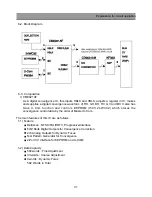
The video signal that is first amplified in PGB processor is input to video AMP in approx. 3.5Vp-
p level. TDA111Q used as a video AMP is a 13Mhz band AMP which outputs a video near to
Vdd according to gain control voltage when Vdd is 200V. The following figure shows the internal
block diagram of TDA6111Q.
Block diagram of TDA6111Q
There are two cathode outputs and a independent feedback output. Low input (Vdd) is 12V and
high input (Vddh) is 200V. A peaking circuit is designed in Amp IC input and output part for high
band compensation. The entire output gain is about 34db.
Summary of Contents for DSJ-4710CRA
Page 23: ...22 Explanation for circuit operation Explanation for circuit operation...
Page 24: ...23 Explanation for circuit operation...
Page 25: ...24 Explanation for circuit operation...
Page 26: ...25 Explanation for circuit operation...
Page 27: ...26 Explanation for circuit operation...
Page 28: ...27 Explanation for circuit operation...
Page 77: ...76 8 Schematic Diagram 1 Block Diagram...
Page 78: ...77 Schematic Diagram 2 Power...
Page 79: ...78 Schematic Diagram 3 REAR IO...
Page 80: ...79 Schematic Diagram...
Page 81: ...80 Schematic Diagram 5 Deflection...
Page 82: ...81 6 Converergence Amp Sound Amp Schematic Diagram...
Page 83: ...82 7 Convergence Module Schematic Diagram...
Page 84: ...83 8 CRT Amp Schematic Diagram...
Page 85: ...84 9 Control Side Schematic Diagram...
Page 86: ...85 1 MAIN PCB 9 PRINTED CIRCUIT BOARD...
Page 87: ...86 2 POWER PCB PRINTED CIRCUIT BOARD...
Page 88: ...87 3 AMP PCB PRINTED CIRCUIT BOARD...
Page 89: ...88 4 CRT PCB PRINTED CIRCUIT BOARD...
Page 90: ...89 5 DEF PCB PRINTED CIRCUIT BOARD...
Page 91: ...90 6 UNION 1 PCB CONTROL SIDE PRINTED CIRCUIT BOARD...
Page 92: ...91 7 UNION 2 PCB CONV MODULE REAR IO PRINTED CIRCUIT BOARD...
Page 93: ...92 1 DSJ 4710 10 EXPLODED VIEW...
Page 94: ...93 2 DSJ 4720 EXPLODED VIEW...
Page 95: ...94 3 DSJ 5510 EXPLODED VIEW...
Page 96: ...95 4 DSJ 5520 EXPLODED VIEW...
Page 97: ......


