- 10 -
APPENDIX
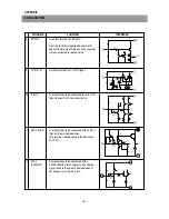
PIN NAME
FUNCTION
INTERFACE
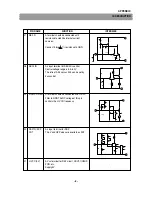
37
DIG.VDD
A Vdd terminal for of digital block.
Supply HVcc voltage through 270 ohms of
resistance.
The voltage of this terminal is clipped to
approximately 3.3V by the internal regulator.
38
SYNC IN
An input terminal for Sync signal.
The input sync tip is clamped by
charging/discharging the coupling capacitors
so as to align the Sync slice level.
Input is through a low impedance buffer,
(input level 1Vp-p/140IRE)
39
Y IN
An input terminal for Y signal.
The pedestal level is clamped by means of
charging/discharging the coupling capacitor,
therefore input through low impedance buffer.
(1Vp-p/140IRE input level)
40
DC RESTOR
A terminal to be connected wiht a capacitor to
detect the average picture level for DC
restoration.
The ratio of the DC restoration is set by bus.
Leave this terminal open if the DC restoration
is not required.
31
30
2.6V
30
H VCC
30
750
37
38
31
33
1k
39
42
19
1k
1k
1k
40
42
19
50k
50k
IC DESCRIPTION
Summary of Contents for DTD-29U8ME
Page 5: ...4 CIRCUIT BLOCK DIAGRAM...
Page 12: ...SCHEMATIC DIAGRAM 11...
Page 13: ...PRINTED CIRCUIT BOARD PCB MAIN 12...
Page 14: ...13 PRINTED CIRCUIT BOARD...
Page 15: ...14 PRINTED CIRCUIT BOARD...
Page 17: ...16 PRINTED CIRCUIT BOARD...
Page 18: ...17 PRINTED CIRCUIT BOARD...
Page 19: ......


