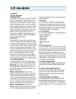
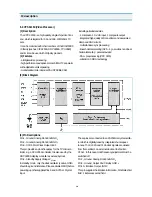
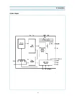
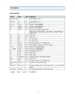
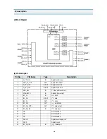
background image

15

(4) PIN DESCRIPTION

Figure 2. Pin Description

IC description

RESET 

Reset 

(input, active low). The ST9+ is initialised 

by the Reset signal. With the deactivation of RESET, 
program execution begins from the Program memory 
location pointed to by the vector contained in program 
memory locations 00h and 01h.

R/G/B 

Red/Green/Blue. 

Video color analog DAC out-

puts

FB 

Fast Blanking. 

Video analog DAC output.

VOD 

Main power supply voltage(5V 10%, digital)

WSCF, WSCR 

Analog pins for the VPS/WPP slicer line 

PLL.

MCFM 

Analog pin for the display pixel frequency multi-

plier.

OSCIN, OSCOUT 

Oscillator 

(input and output).

These pins connect a parallel-resonant crystal(24MHz 
maximum), or an external source to the on-chip clock 
oscillator and buffer. OSCIN is the input of the oscilltor 
inverter and internal clock generator; OSCOUT is the 
output of the oscillator inverter.

VSYNC 

Vertical Sync. 

Vertical video synchronisation 

input to OSD. Positive or negative polarity.

HYNC/CSYNC 

Horizontal/Composite sync. 

Horizontal 

or composite video synchronisation input to OSD. Posi-
tive or negativety.

PXFM 

Analog pin for the Display Pixel Frequency Multi-

plier

AVDD 

Analog VDD of PLL. 

This pin must be tied to 

VDD externally to the ST92195.

GND 

Digital circuit ground.

AGND 

Analog circuit ground(must be tied externally to 

digital GND).

CVBS1 

Composite video input signal for the Teletext 

slicer and sync extraction.

CVBS2 

Composite video input signal for the VPS/WSS 

slicer. Pin AC coupled.

AVDD1, AVDD2 

Analog power supplies(must be tied 

externally to AVDD).

TXCF 

Analog pin for the VPS/WSS line PLL.

CVBSO, JTDO, JTCK 

Test pins : leave floating.

JTMS, TEST0 

Test pins : must be tied to AVDD2.

JTRST0 

Test pin : must be tied to GND.

Summary of Contents for DTJ-28G8F

Page 1: ...Service Manual 66 Cm STEREO Colour Television CHASSIS CP 810 DAEWOO ELECTRONICS CO L TD http svc dwe co kr MAR 2000 MODEL DTJ 28A6F DTJ 28A7F DTJ 28B1F DTJ 28G6F DTJ 28G7F DTJ 28G8F S M No CP810P 010...

Page 2: ...cifications 3 3 Circuit block Diagram 5 4 Alignment Instructions 6 5 IC Description 12 6 IC DC Voltage Charts 32 7 Service Parts List Recommendable Spare Parts List 35 8 Mechanical Exploded View 45 9...

Page 3: ...tial of the picture tube before handling the tube The picture tube is highly evacuated and if broken glass fragments will be violently expelled 2 If any Fuse in this TV receiver is blown replace it wi...

Page 4: ...rograms Aux Terminal 21 pin EURO SCART jack AV input TV output RGB input 21 pin EURO SCART jack AV input S VHS input RCA type AV input jack Headphone jack 3 5 mm JACK AUDIO TERMINAL AUDIO OUT L R Remo...

Page 5: ...5Vrms Imp 10 k RF 60 MOD 7 Blue in 0 7Vpp 2dB Imp 75 8 Slow Function Switching TV 0 2V PERI 9 5 12V Imp 10 k 9 Green Earth 10 NC 11 Green In 0 7Vpp 2dB Imp 75 12 NC 13 Red Earth 14 Rapid Blanking Swit...

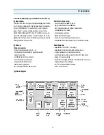
Page 6: ...5 3 Circuit Block Diagram...

Page 7: ...6 4 Alignment Instructions 4 1 User Remocon R 22D05...

Page 8: ...7 R 23D05 Alignment Instructions...

Page 9: ...tons on the remote controller are used to move the selection bar up or down the Menus 6 The VOL UP DOWN buttons on the remote controller are used to adjust levels 7 If you want to exit from Service Mo...

Page 10: ...nerator with RF Frequency 210 25MHz 10CH Pattern RETMA 2 Selectthe G2 inMenu 3 And a Horizontal Line will appear on the screen 4 Adjust the SCREEN VOLUME on FBT barely to see the Horizontal Line 5 Pre...

Page 11: ...t picture centering with the select H Center by volume UP DOWN keys 4 7 EW 4 7 1 WIDTH 1 Apply a RETMA PATTERN Signal 2 Adjust the horizontal width to make a perfect circle with the select H Width by...

Page 12: ...to be on the center position 4 9 SUB BRIGHT 4 9 1 Pattern Retma 4 9 2 Adjust the SUB BRIGHT with the select Sub Bri by volume UP DOWN keys so that only H Center parts of picture can be seen 4 10 DOUBL...

Page 13: ...interrupt controller keep running at a frequency programmable via the CCU In this mode the power consumption of the device can be reduced by more than 95 LP WFI Wait For Interrupt Mode The Wait For In...

Page 14: ...M TeletextandDisplayRAM 56 lead Shrink DIP package 28fullyprogrammableI Opins Serial Peripheral Interface FlexibleClockcontrollerforOSD DataSlicerandCore clocks running from one single low frequency e...

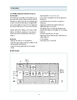
Page 15: ...14 3 Block Diagram IC description...

Page 16: ...put of the oscilltor inverter and internal clock generator OSCOUT is the output of the oscillator inverter VSYNC Vertical Sync Vertical video synchronisation input to OSD Positive or negative polarity...

Page 17: ...ssing VPC 3215 submicronCMOStechnology Pin 1 Ground Analog Front End GND Pin 2 Ground Analog Front End GND Pin 3 CCU 5 MHz Clock Output CLK5 This pin provides a clock frequency for the TV microcon tro...

Page 18: ...face allows digital switching of up to 8 sources to the back end processor Switching for different sources is prioritized and can be on a per pixel basis Pin 51 Ground Output Pad Circuitry GND Pin 52...

Page 19: ...d 2 Feature analog input for RGB or YUV and Fast Blank triple 8 bit analog to digital converters for RGB YUV with internal programmable clamping single 6 bit analog to digital converter for Fast Blank...

Page 20: ...RC4 carry the halfbyte nibble multiplex format In a stand alone application where the CIP 3250A serces as an AD converter these are the outputs for the digital Red sig nal pure binary or the digital c...

Page 21: ...d pins of the chip i e 18 52 58 60 62 64 66 and68 mustbeconnectedtogetherlowresistive The layout of the PCB must take into consideration the need for a low noise ground Pin 59 ADREF Connect External C...

Page 22: ...connected together low rresistive The layout of the PCB must take into consideration the need for a low noise ground Pin67 RVAnalogRed VChromaInput This input pin takes the AC coupled analog componen...

Page 23: ...s complement or unsigned Color difference output data representation 2 s complement or unsigned Sync Generation for backend IC Bus control 400 kHz P MQFP 64 package 5V 5 supply voltage 2 General Descr...

Page 24: ...23 3 Block Diagram IC description...

Page 25: ...20 SCL I Bus clock line 19 TESTIN I TTL Test input connect to for normal operation 18 TESTEN I TTL Test enable input connect to for normal operation 13 10 UVOUT4 O TTL Data output UV see data format...

Page 26: ...ng soft limiter gamma correction color transient improvement programmable RGB matrix picture frame generator two analog RGB Fast Blank inputs Deflection processing scan velocity modulation output high...

Page 27: ...cture tube from burn in in the event of a malfunction of the vertical deflection stage If the peak to peak value of the vertical sawtooth signal is too small the RGB output signals are blanked Pin 12...

Page 28: ...required Pin 30 34 Fast Blank InputFBLIN1 2 These pins are used to switch the RGB outputs to the externalanalogRGBinputs FBLIN1switchestheRIN1 GIN1 and BIN1 inputs FBLIN2 switches the RIN2 GIN2 and BI...

Page 29: ...the vertical sync informatoion Either single or double vertical frequency or VGA vertical sync signal Pin 65 66 Crystal Output Input XTAL2 XTAL1 These pins are connectecd to an 5 MHz crystal oscillat...

Page 30: ...surround delay according to table created by Dolby Labortories 1 ms steps 2 input channels e g MSP and DRPA 2 output channels freely programmable with sound channels L R resp L C R C C S Sub or input...

Page 31: ...ital control IO 0 5 ADR_SEL IN Bus address select 6 STANDBYQ IN Standby low active 7 I2C_CL IN clock 8 I2C_DA IN OUT data 9 I2C_CL OUT clock 10 I2C_WS OUT wordstrobe 11 I2C_DA_OUT1 OUT data output 12...

Page 32: ...CAPL_C2 18 NC Volume capacitor Channel2 33 20 19 AHVSUP 18 NC Analog power supply 8V 34 20 19 CAPL_C1 18 NC Volume capacitor Channel1 35 20 19 AHVSS 18 NC Analog ground 36 20 19 AGNDC 18 NC Analog ref...

Page 33: ...1 12 13 14 15 16 17 18 19 20 V DC 2 4 2 4 2 4 0 5 0 6 0 6 0 5 4 9 0 1 3 Pin No 21 22 23 24 25 26 27 28 29 30 V DC 0 4 0 4 0 3 4 9 0 7 0 7 0 0 08 0 08 0 Pin No 31 32 33 34 35 36 37 38 39 40 V DC 0 08 1...

Page 34: ...0 6 2 1 0 8 Pin No 31 32 33 34 35 36 37 38 39 40 V DC 5 0 5 0 0 8 1 6 0 0 0 2 0 5 0 0 6 Pin No 41 42 43 44 45 46 47 48 49 50 V DC 0 0 0 0 1 5 0 0 0 0 0 2 3 Pin No 51 52 53 54 55 56 V DC 2 3 5 0 5 0 0...

Page 35: ...DC 2 2 2 1 Pin No 1 2 3 4 5 6 7 8 9 10 V DC 3 2 12 2 3 2 3 2 210 0 0 6 172 0 0 115 0 177 0 Pin No 11 12 13 14 15 V DC 0 6 119 0 168 0 0 6 116 0 Pin No 1 2 3 4 5 6 7 8 9 10 V DC 0 5 0 1 0 1 0 0 1 9 0 0...

Page 36: ...SK FRONT AS DTJ 28A6F M201 4852074501 MASK FRONT HIPS BK M251 4852540601 GRILL L PS SHEET M252 4852538401 GRILL R PS SHEET ZZ220 PTSPPWD228 SPEAKER AS DTJ 28G6F R R is recommendable spare part is safe...

Page 37: ...01V C ELECTRO 25V RSS 100MF 6 3X11 TP LOC PART CODE PART NAME DESCRIPTION REMARK Service Parts List Recommendable Spare Parts List C826 CEXF1E101V C ELECTRO 25V RSS 100MF 6 3X11 TP C827 CEXF1E471C C E...

Page 38: ...C673 HCTAD100MB C CHIP TANTAL 10V 10MF M 3216 CC676 HCTAD479MB C CHIP TANTAL 10V 4 7MF M 3216 CC677 HCTAD479MB C CHIP TANTAL 10V 4 7MF M 3216 LOC PART CODE PART NAME DESCRIPTION REMARK Service Parts L...

Page 39: ...T CODE PART NAME DESCRIPTION REMARK Service Parts List Recommendable Spare Parts List DA20 DUZ5R6BM DIODE ZENER UZ 5 6BM TAPPING DA21 DUZ5R6BM DIODE ZENER UZ 5 6BM TAPPING DA22 DUZ5R6BM DIODE ZENER UZ...

Page 40: ...MM L608 5CPZ109M02 COIL PEAKING 1UH M AXIAL 3 5MM L609 5MC0000100 COIL BEAD HC 3550 LOC PART CODE PART NAME DESCRIPTION REMARK Service Parts List Recommendable Spare Parts List L610 58C0000116 COIL BE...

Page 41: ...ART CODE PART NAME DESCRIPTION REMARK Service Parts List Recommendable Spare Parts List R417 RF 4Y228K R FUSIBLE 1 4 0 22 OHM K R418 RF01Z188K R FUSIBLE 1W 0 18 OHM K TAPPING R420 RN02B473JS R METAL F...

Page 42: ...0 OHM J 2012 LOC PART CODE PART NAME DESCRIPTION REMARK Service Parts List Recommendable Spare Parts List RC411 HRFT123JCA R CHIP 1 10 12K OHM J 2012 RC412 HRFT101JCA R CHIP 1 10 100 OHM J 2012 RC413...

Page 43: ...101090 SW TACT SKHV17910A SW703 5S50101090 SW TACT SKHV17910A LOC PART CODE PART NAME DESCRIPTION REMARK Service Parts List Recommendable Spare Parts List SW704 5S50101090 SW TACT SKHV17910A SW801 5S4...

Page 44: ...CERA 50V X7R 1200PF K 2012 CCS06 HCBK472KCA C CHIP CERA 50V X7R 4700PF K 2012 CCS07 HCQK101JCA C CHIP CERA 50V CH 100PF J 2012 CCS08 HCQK101JCA C CHIP CERA 50V CH 100PF J 2012 JCD01 HRFT000 CA R CHIP...

Page 45: ...392JCA R CHIP 1 10 3 9K OHM J 2012 RCS13 HRFT273JCA R CHIP 1 10 27K OHM J 2012 RCS14 HRFT563JCA R CHIP 1 10 56K OHM J 2012 RCS15 HRFT100JCA R CHIP 1 10 10 OHM J 2012 RCS16 HRFT820JCA R CHIP 1 10 82 OH...

Page 46: ...11 13 12W8OHMSP 58126F 2 SPEAKER 4858311110 12 SW PA 1 SPRING 4856716000 11 CR 4 WASHER RU BBER 4856215402 10 SW RM SK 5 YL 4 SCREW_CRT _F IX 4856015820 9 PVC 1 DECO C TRL 4855059501 8 HIPS BK 1 BUTT...

Page 47: ...66ECY13X_26V 15 SWRM BK SCREW TAPPING 7128301212 14 SWRM BK SCREW TAPPING 7122401612 13 SWRM BK SCREW TAPPING 7122401212 12 POM N6 N66 G30 DOOR LOCK 4857923300 11 SWPA SPRING 4856716000 10 CR T2 0 WAS...

Page 48: ...GY T T2 R N D 3X 10 M FZN A L EX P FC 5 00 0 0 70 2 C P 8 10 P P B K A L SIL VE R S WP A P IE 0 5 A BS GY P S P H ILIP S 2 8 S WR M SK5 L 35 C R T2 0 A BS GY T 2S WAS 3X 1 0 M FZN 1 1 1 0 9 8 7 6 5 4...

Page 49: ...485 2821501 SWRM BK 2 SCREW TAPPING 7121301212 SWRM BK 10 SCREW TAPPING 712 2401612 SWRM SK 5 BK 4 SCREW_CRT_FIX 485 6015800 CR 4 WASHER RUBBER 485 6215402 SWPA 1 SPRING 4856716001 A1050P H24 1 MARK B...

Page 50: ...49 Mechanical Exploded View 5 DTJ 28G7F...

Page 51: ...6 7 8 9 10 11 13 14 15 16 19 20 21 CLOTH BLACK 4857818702 FELT T0 7 L 250 W 15 2 7122401212 8 PCB A ss cp 776 1 A66EAK071X11 CRT A ss 1 GLASS 4857817610 CLOTH BLACK 3 FELT 300X20X0 7 HIPS BK 48556161...

Page 52: ...51 10 Printed Circuit Board...

Page 53: ......

Page 54: ...DAEWOO ELECTRONICS CO LTD 686 AHYEON DONG MAPO GU SEOUL KOREA C P O BOX 8003 SEOUL KOREA TELEX DWELEC K28177 8 CABLE DAEWOOELEC E mail leesk web dwe co kr FAX 82 2 360 7802 TEL 82 2 360 7877...

Reviews: