


17
IC description
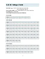
2
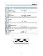
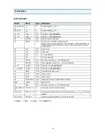
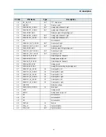
Pin 12 - Vertical Sync Pulse, VS
This pin supplies the vertical sync signal.
Pin 13 - Front Sync Pulse, FSY
This pin supplies the front sync information.
Pin 14 - Main Sync/Horizontal Sync Pulse MSY/HS
This pin supplies the horizontal sync pulse information in
line-locked mode. In DIGIT3000 mode, this pin is the main
sync input.
Pin 15 - Helper Line Output, Helper
This signal indicated a helper line in PAL + mode.
Pin 16 - Horizontal Clamp Pulse, HC
This signal can be used to clamp an external video signal,
that is synchronous to the input signal. The timing is pro-
grammable.
Pin 17 - Active Video Output, AVO
This pin indicates the active video output data. The signal
is clocked with the LLC1 clock.
Pin 18 - Double Output Clock, LLC2
Pin 19 - Output Clock, LLC1
This is the clock reference for the luma, chroma, and sta-
tus outputs.
Pin 26 - Ground, Output Pad Circuitry GND
Pin 20 to 25,28,29 - Luma Output Y0-Y7
These output pins carry the digital luminance data. The
data are clocked with the LLC1 clock.
Pin 30 - Main Clock Output CLK20
This is the 20.25MHz main clock output.
Pin 31 - Supply Voltage, Digital Circuitry V
Pin 34 - Ground, Digital Circuitry GND
Pin 35 - Ground, Output Pad Circuitry GND
Pin 36 - Supply Voltage, Output Pad Supply V
Pin 38 to 43,46,47 - Chroma Outputs C0-C7
These outputs carry the digital CrCb chrominance data.
The data are clocked with the LL1 clock. The data are
sampled at half the clock rate and multiplexed. The CrCb
multiplex is reset for each TV line.
Pin 48 to 50 - Picture Bus Priority PR0-PR2
The Picture Bus Priority lines carry the digital priority
selection signals. The priority interface allows digital
switching of up to 8 sources to the back-end processor.
Switching for different sources is prioritized and can be on
a per pixel basis.
Pin 51 - Ground, Output Pad Circuitry GND
Pin 52 - VGAV-Input.
This pin is connected to the vertical sync signal of a VGA
signal.
Pin 53 - Front-End/Back-End Data FPDAT
This pin interfaces to the DDP 3300A back-end processor.
The information for the deflection drives and for the white
drive control, i.e. the beam current limiter, is transmitted by
this pin.
Pin 54 - Reset Input RESQ
A low level on this pin resets the VPC 32xx.
Pin 55 - Bus Data SDA
The pin connects to the bus data line.
Pin 57 - Test Input TEST
This pin enables factory test modes. For normal operation,
it must be connected to ground.
Pin 59 - Ground, Analog Front-End GND
Pins 62,61,60,58 - Video 1-4
These are the analog video inputs. A CVBS or S-VHS
luma signal is converted using the luma (Video 1) AD con-
verter. The VIN1 input can also be switched to the chroma
(Video 2) ADC. The input signal must be AC-coupled.
Pin 63 - Chroma Input CIN
This pin is connected to the S-VHS chroma signal. A resis-
tive divider is used to bias the input signal to the middle of
the converter input range. CIN can only be connected to
the chroma (Video 2) A/D converter. The signal must be
AC-coupled.
Pin 64 - Analog Video Output, VOUT
The analog video signal that is selected for the main
(luma, CVBS) ADC is output at this pin. An emitter follower
is required at this pin.
Pin 65 - Ground, Analog Shield Front-End GND
Pin 66 - Supply Voltage, Analog Front-End V
Pin 67 - Signal GND for Analog Input ISGND
This is the high quality ground reference for the video
input signals.
Pin 68 - Reference Voltage Top VRT
Via this pin, the reference voltage for the A/D converters is
decoupled. The pin is connected with 10uF/47nF to the
Signal Ground Pin.
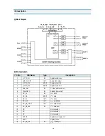
P
SUPD
D
P
SUPP
P
I C
2
I C
2
Summary of Contents for DTJ-28G8F
Page 6: ...5 3 Circuit Block Diagram...
Page 7: ...6 4 Alignment Instructions 4 1 User Remocon R 22D05...
Page 8: ...7 R 23D05 Alignment Instructions...
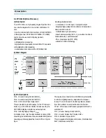
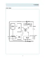
Page 15: ...14 3 Block Diagram IC description...
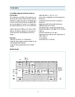
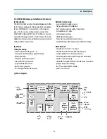
Page 24: ...23 3 Block Diagram IC description...
Page 50: ...49 Mechanical Exploded View 5 DTJ 28G7F...
Page 52: ...51 10 Printed Circuit Board...
Page 53: ......