
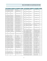
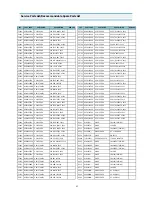
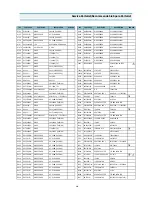
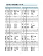
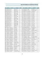

30
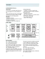
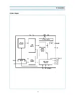
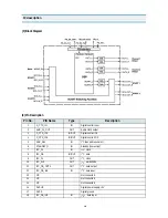
IC description
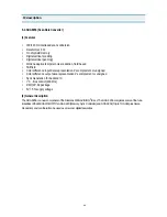
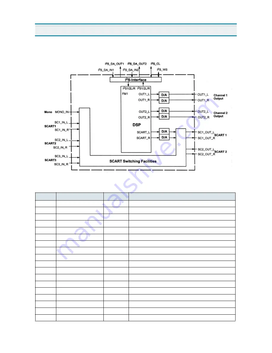
(3) Block Diagram
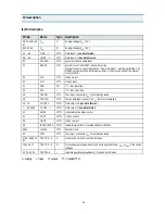
(4) Pin Description
Pin No.
PIN Name
Type
Description
1
D_CTR_IN
IN
Digital control input
2
AUD_CL_OUT
OUT
Audio clock output
3
D_CTR_IO1
IN/OUT
Digital control IO1
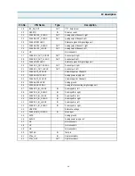
4
D_CTR_IO1
IN/OUT
Digital control IO 0
5
ADR_SEL
IN
-Bus address select
6
STANDBYQ
IN
Standby (low-active)
7
I2C_CL
IN
clock
8
I2C_DA
IN/OUT
data
9
I2C_CL
OUT
clock
10
I2C_WS
OUT
wordstrobe
11
I2C_DA_OUT1
OUT
data output
12
I2C_DA_IN1
IN
data input
13
NC
Not connected
14
NC
Not connected
15
NC
Not connected
16
DVSUP
Digital power 5V
17
DVSS
Digital ground
18
I2S_DA_IN2
IN
- data input
I C
2
I C
2
I C
2
I C
2
I C
2
I C
2
I C
2
I S
2 2
Summary of Contents for DTJ-28G8F
Page 6: ...5 3 Circuit Block Diagram...
Page 7: ...6 4 Alignment Instructions 4 1 User Remocon R 22D05...
Page 8: ...7 R 23D05 Alignment Instructions...
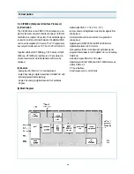
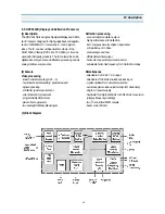
Page 15: ...14 3 Block Diagram IC description...
Page 24: ...23 3 Block Diagram IC description...
Page 50: ...49 Mechanical Exploded View 5 DTJ 28G7F...
Page 52: ...51 10 Printed Circuit Board...
Page 53: ......