background image

- 13 -

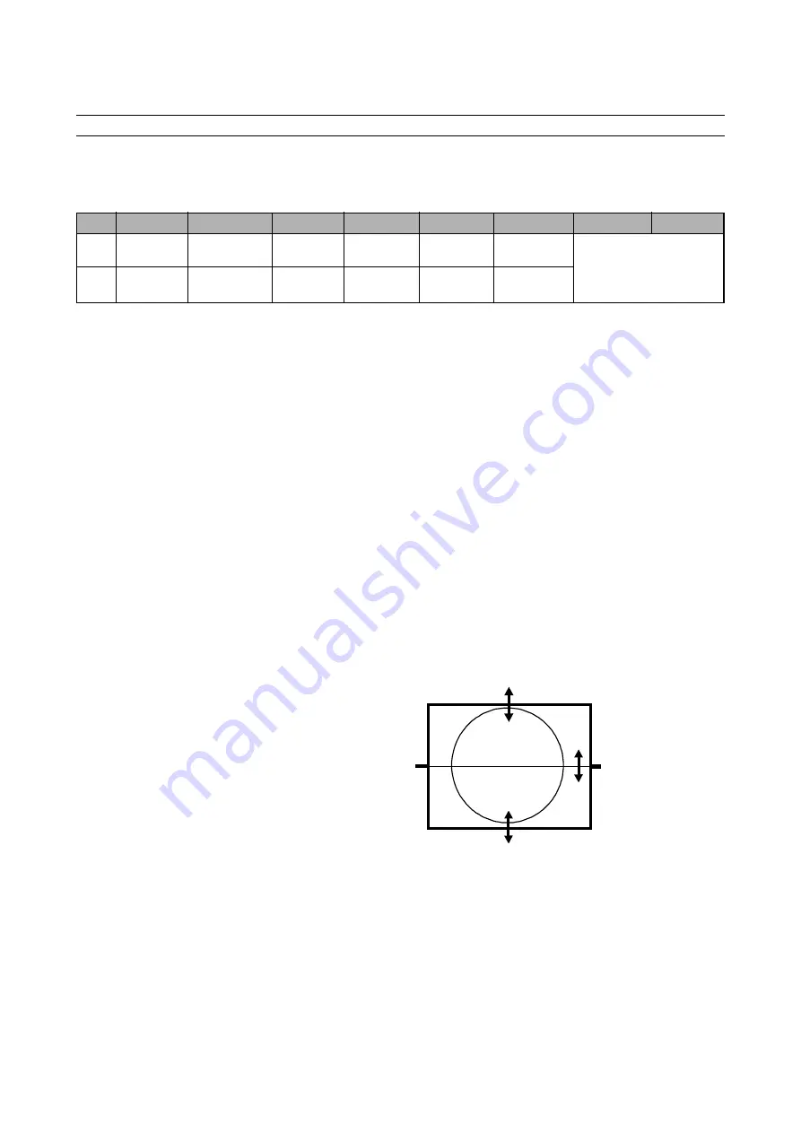
3-3 Microcontroller con figuration : Option bits
These option bits are  availa ble from Ser vice mode. First find the OPTION control, and then use keys 0...7 on the
remote keypad to control bits 0 to 7 respect ively. The table below shows the options availa ble ;

B7 B6 B5 B4 B3 B2 B1 B0

TOP text FASTEXT SVHS3

off /FLOF off disable

TOP text FASTEXT SVHS3

on (FLOF) on enable

1

0

TUBE 4:3

TUBE 16:9

X

X

X

X

Tuner options
00 = Philips
01 = ALPS
10 = Philips ( AGC intern)
11 = Not used.

Set all the unused bits, marked ‘X’, to be 0 for future compatibility.

3-4 TV set Alignment
3-4-1- Local oscillator alignment
Tune a colour bar pattern . The frequency of the signal carrier must be accurate ( Max +/- 10Khz  d eviation from the
nominal channel frequency).
Find “AFT” item in service mode .
Adjust the coil L150 to bring the cursor to central position : 32.

3-4-2- G2 alignment
- Tune a colour bar pattern.
- Find the “G2 - SCREEN ” item in service mode.
- Adjust screen volume ( on FBT ) to bring the cursor to central position : 32.

3-4-3- White balance
- Select a dark picture and adjust RED BIAS and GRN BIAS to the desired colour temperature.
- Select a bright picture and adjust RED, GRN and BLUE GAIN to the desired colour temperature.

3-4-4- Focus
Adjust the Focus volume ( on FBT ) to have the best resolution on screen.

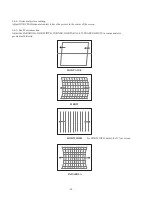
3-4-5- Vertica l geometry
Adjust V.LINEAR (linear ity), S CORRECT
(S. Correction), VERT SIZE (Vertical
amplitude), VERT CENT (v ertical cent ring)
to compensate for vertical distortion.

Summary of Contents for DTP-28B1

Page 1: ...Service Manual S M No TWP895BEF0 DAEWOO ELECTRONICS CO LTD http svc dwe co kr AUG 2001 ColourTelevision CHASSIS WP 895 MODEL DTP 28B1...

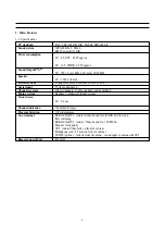
Page 2: ...overage Off air channels S cable channels and hyperband Tuning system frequency synthesiser tuning system Visual screen 28 66 cm Channel indication On Screen Display Program Selection 100 programmes A...

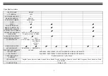
Page 3: ...TS OFF SPATIAL OFF SPATIAL PANORAMA VIRTUAL DOLBY GRAPHIC EQUALIZER AV3 AUDIO INPUT DEDICATED DEDICATED TELETEXT PAGE MEMORY 10 PAGE TOP TELETEXT AVAILABLE SELECTABLE IN FACTORY SERVICE MODE BY OPTION...

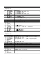
Page 4: ...dance 75 16 Fast Switching 0 to 0 4V Logic 0 1 to 3V Logic 1 Impedance 75 17 Video Out Earth 18 Video In Earth 19 Video Output 1 Vpp 3dB Impedance 75 20 Video Input 1 Vpp 3dB Impedance 75 21 Common Ea...

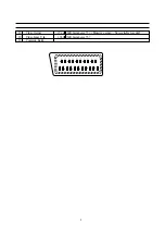
Page 5: ...5 19 Video Output 1 Vpp 3dB Impedance 75 Monitor output Not available for cp885 20 Video Input Y In 1 Vpp 3dB Impedance 75 21 Common Earth...

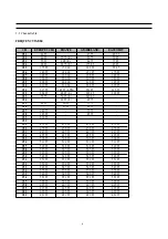
Page 6: ...85 75 C19 201 25 C20 C21 471 25 471 25 471 25 471 25 C22 479 25 479 25 479 25 479 25 C23 487 25 487 25 487 25 487 25 C24 495 25 495 25 495 25 495 25 C25 503 25 503 25 503 25 503 25 C26 511 25 511 25 5...

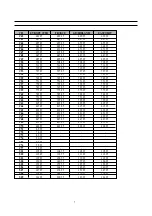
Page 7: ...25 767 25 767 25 767 25 C59 775 25 775 25 775 25 775 25 C60 783 25 783 25 783 25 783 25 C61 791 25 791 25 791 25 791 25 C62 799 25 799 25 799 25 799 25 C63 807 25 807 25 807 25 807 25 C64 815 25 815 2...

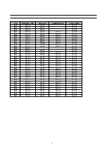
Page 8: ...11 25 S23 319 25 319 25 319 25 319 25 S24 327 25 327 25 327 25 327 25 S25 335 25 335 25 335 25 335 25 S26 343 25 343 25 343 25 343 25 S27 351 25 351 25 351 25 351 25 S28 359 25 359 25 359 25 359 25 S2...

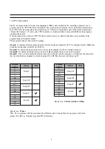
Page 9: ...lected country and named by the TV controlling softw are Within this group the sorting order is fixed by the A TSS list Group II It contains all the pro grams with a strong signal strength which are n...

Page 10: ...nd then a second time with France system selected positive video modulation Special case GB Note for sa tellite recei ver users Before starting ATSS tur n On your satellite r ecei ver and tune SKY NEW...

Page 11: ...2 Discharge the high potential of the picture tube before handling the tube The picture tube is highly evacuated and if broken glass fragments will be violently expelled 2 If any Fuse in this TV recei...

Page 12: ...menu key or Std By key 3 2 Service mode navigation Pr Up Down remote keys cycle through the service items available Vol remote keys Decrement Increment the values within range 0 7 digit keys Toggle b...

Page 13: ...he frequency of the signal carrier must be accurate Max 10Khz d e viation from the nominal channel frequency Find AFT item in service mode Adjust the coil L150 to bring the cursor to central position...

Page 14: ...centring Adjust HOR CEN Horizontal center to have the picture in the center of the screen 3 4 7 Eau West comection Adjust the PARABOLA HOR WIDTH CORNER HOR PARAL EW TRAPEZ H BOW to compensate for geo...

Page 15: ...15 CORNER EW TRAPEZ 3 4 8 AGC Adjust the antenna signal level at 70 dB V 2 Tune a colour bar pattern Find the AGC item in service mode Adjust AGC volume RB10 to bring the cursor to central position 32...

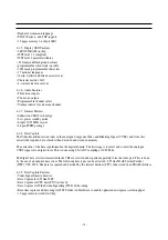
Page 16: ...bit Controller 4 1 1 Block diagram of the VCT 4 1 2 TV signal Processor Four composite video inputs two S VHS inputs AnalogueYC r C b input Composite video monitor Multistandard colour decoder 1 cryst...

Page 17: ...are module watchdog timer 14 bit PWM for voltage synthesis Four 8 bit PWMs 10 bit ADC with 15 1 input MUX I2C bus master interface 24 programmable I O ports 80C51 controller core standard instruction...

Page 18: ...l CVBS and from this extracts the required data which is then decoded and stored in memory The extraction of the data is performed in the digital domain The first stage is to select and convert the an...

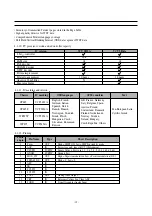
Page 19: ...r 4 1 11 IC marking and version Chassis OSD languages ATSS countries Text CP885 VCT3832A CP885F VCT3834A WP895F VCT3834A WP895 VCT3834A Pan European Latin Cyrillic Greek GB France Germany Italy Belgiu...

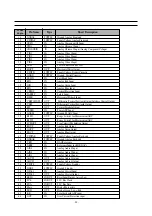
Page 20: ...t 36 EW OUT Vertical Parabola Output 37 SENSE IN SenseADC Input 38 GNDM SUPPLY Ground MADC Input 39 RSW1 OUT Range Switch1 for MeasurementADC 40 RSW2 OUT Range Switch2 for MeasurementADC 41 SVMOUT OUT...

Page 21: ...GND GND XREF VRD GND 5V B out G out R out SVM out RSW2 RSW1 GND SENSE EW VERTQ VERT HFLB Power 1 2 3 4 5 7 8 9 10 17 19 20 21 22 23 24 25 26 27 28 29 31 30 32 18 11 12 13 14 15 16 6 AGC S B 5V Gnd MOD...

Page 22: ...TV sound standards Precise bit error rate indication Automatic switching from NICAM to FM AM or vice versa Improved NICAM synchronisation algorithm Improved carrier mute algorithm Improved AM demodul...

Page 23: ...h and French TV standards high quality stereo sound is transmitted digitally The systems allow two high quality digital sound channels to be added to the already existing FM AM channel The sound codin...

Page 24: ...6 5 6 2578125 D K1 FM Stereo SECAM East USSR 6 5 6 7421875 D K2 6 5 5 85 D K NICAM FM Mono NICAM Hungary Architecture of MSP341x Pin connections and short description Pin No Pin Name Type Short descr...

Page 25: ...ground 1 high voltage part 36 SC1_OUT_R Out Scart output 1 right 37 SC1_OUT_L Out Scart output 1 left 38 NC Not Connected 39 AHVSUP Analog power supply 8 0V 40 CAPL_M Volume capacitor MAIN 41 AHVSS An...

Page 26: ...nt free AFC without external reference circuit polarity of the AFC curve is switchable VIF AGC for negative modulated signals peak sync detection and for positive modulation peak white black level det...

Page 27: ...nput symmetrical 4 3 4 Block diagram Offset 26 18 20 21 14 VCO l switch VCO Control phase shift FPLL VIF amp Loop filter comp optional 4 9 16 AM det FM det 25 24 17 Cref 23 13 22 19 6 7 8 15 11 10 27...

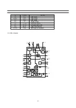
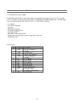
Page 28: ...xJ Stereo AudioAmplif ier The TDA8944J TDA 8946J is a dual channel audio po wer amplifier with an output power of 2 x 7W 2 X 15W at an 8 load and a 12V supply The circuit contains two Bridges Tied Loa...

Page 29: ...29 Block diagram TDA8944J...

Page 30: ...Bipolar CMOS and DMOS devices MOS transistors are used in the output stage because of the absence of second breakdown 4 5 1 TDA8357J Features Few external components High efficient fully DC coupled ve...

Page 31: ...the diode modulator circuit Features Few external components Highly efficient fully DC coupled vertical output bridge circuit Short rise and fall time of the vertical flyback switch Guard circuit Tem...

Page 32: ...32...

Page 33: ...idth of 5 5 MHz for an output signal of 60 Vpp High slew rate of 900V s No external components required Very simple application Single supply voltage of 200V Internal reference voltage of 2 5 V Fixed...

Page 34: ...34 Block diagram TDA6107Q...

Page 35: ...k 7 WC Write control 8 Vcc Supply voltage 4 Vss Ground The memory device is compatible with the I2C memory standard This is a two wire serial interface that uses a bi directionnal data bus and serial...

Page 36: ...IC designed for flyback converter type switch mode power supply applications 4 8 2 Features Small SIP fully isolated molded 5 pins package Many protection functions Pulse by pulse overcurrent protecti...

Page 37: ...rent in 4 5 IIN on 30 mA operation Circuit current in non 4 5 IIN off 100 mA A operation Maximum OFF time TOFF max 45 55 SEC Minimum time for input of 1 5 TTH 2 1 0 SEC quaxi resonant signals Minimum...

Page 38: ...haracteristics IC PINS RATING NUMBER MIN TYPE MAX Drain to source break 3 2 VDSS 650 V voltage Drain leakage current 3 2 IDSS 300 A On resistance 3 2 RDS on 1 95 Switching time 3 2 tf 2 50 noec Therma...

Page 39: ...39 5 Circuit description 5 1 Block diagram...

Page 40: ...Pin 6 7 of the VIF amplifier 5 2 2 Vision IF Amplifier This amplifier consists of three AC coupled amplifier stages Each differential amplifier is gain controlled by the automatic gain control circui...

Page 41: ...generate the tuner AGC current at Pin 11 open collector output The take over point of the tuner AGC can be adjusted at Pin 10 by a potentiometer or an external dc voltage from interface circuit or mi...

Page 42: ...ated to the average level of AM or FM carrier and controls the SIF amplifier to provide a constant SIF signal to the AM demodulator and QPS mixer 5 2 7 Quasi Parallel Sound QPS Mixer The QPS mixer is...

Page 43: ...nance signal These inputs are internally biased and have a fixed gain amplifier 5 3 4 Clamping The composite video input signals are AC coupled to the IC The clamping voltage is stored on the coupling...

Page 44: ...rds The colour killer uses the burst phase burst frequency measurement to identify a PAL NTSC or SECAM colour signal For PAL NTSC the colour is switched off killed as long as the colour subcarrier PLL...

Page 45: ...are converted by a program mable matrix to RGB colour space The digital OSD insertion circuit allows the insertion of a 5 bit OSD signal The OSD signals and the display clock are synchronised to the h...

Page 46: ...ted drives and brightness 5 3 17 Analogue RGB Insertion The VCT 38xxA allows insertion of external analogue RGB signals The RGB signal is key clamped and inserted into the main RGB by the Fast Blank s...

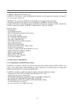
Page 47: ...P D 5 4 Microcontroller 5 4 1 Introduction The TV controller basically consists of the CPU RAM ROM and a number of peripheral modules For instance a memory banking module is included to allow access t...

Page 48: ...for the analogue to digital converter Controller I O pin configuration and function table pin name description To reduce power consumption in stand by mode all ports not used are configured in high im...

Page 49: ...error typically 8 linear ZOOM 16 9 133 100 Picture is displayed 16 9 picture letter box filling the full screen format with 430 active width and height lines PANORAMA 100 100 Picture is displayed Used...

Page 50: ...4 S SW 1 or S SW 2 represent the SLOW SWITCHING inputs of the first SCART AV 1 or second SCART AV 2 these each being pin number 8 5 F SW 1 represents the FAST SWITCHING input of the first SCART AV 1 o...

Page 51: ...ter the intended language that the teletext page should be displayed in As there are only 3 bits there are only 8 codes available to cover all the possible language combinations This means that for a...

Page 52: ...Dutch Danish Finnish Norwegian Swedish Greek Polish Hungarian Czech Slovakian Rumanial Russian 5 6 Sound processing 5 6 1 Analogue sound IF input section The input pins ANA_IN1 and ANA_IN offer the po...

Page 53: ...automatically switches to the analogue sound carrier 1 if the transmission quality is too poor To avoid unwanted automatic switching the threshold levels mono to stereo and stereo to mono are differe...

Page 54: ...deflection coils measured as voltage across R398 which provides internal feedback information The voltage across R398 is proportional to the output current 5 8 1 Flyback voltage The flyback voltage i...

Page 55: ...or flyback converter type switch mode power supply applications 5 9 2 Power supply primary part operations An oscillator generates pulses signals which turn on and off a MOSFET transistor 5 9 2 1 Star...

Page 56: ...ncrease to the set voltage immediately after the control circuit starts operating VIN starts dropping However as this winding voltage reaches the set value before VIN voltage drops to the shutdown vol...

Page 57: ...57 5 9 2 2 STR F6654 oscillating operation...

Page 58: ...d R1 is the OFF time of the MOSFET When C1 voltage falls to around 3 7V the STR F6654 internal oscillator is reversed again and the MOSFET turns ON C1 is quickly charged to around 6 5V The MOSFET cont...

Page 59: ...s regulator provides 5V 3 3V DC voltage to I501 microcontroller power supply pins pin 3 pin 54 and to the reset pulse circuit which provides reset pulse to I501 microcontroller reset pin pin 58 Then t...

Page 60: ...he microcontroller switches TV set to stand by mode decreasing power pin voltage pin 1 5 10 2 TV normal run and stand by mode operations Depending on remote control commands I501 microcontroller part...

Page 61: ...nd I810 controlled rectifier gate pin is set to low no conducting So current from 14V DC voltage from T801 SMPS transformer pin 13 does not flow through Q811 and Q810 transistors but flows through I80...

Page 62: ...error amplifier I806 which corrects unexpected DC voltage variations on this line power supply IC delivery during TV set normal run power supply line IC power supply delivery Remarks 143V FBT FBT sup...

Page 63: ...M PS TRANS I501 MAIN IC OCP FB D801 D804 GRAETZ BRIDGE 16 D821 I810 controlled rectifier HIGH C841 C840 R713 1 3 1 2 61 64 56 54 7 63 CONDUCTING IR IN com supply voltage KEY IN POWER R888 C888 Q809 Q8...

Page 64: ...in is set to high and I810 is conducting So current flows from pin 16 SMPS transformer to the ground via I804 optocoupler and Q810 and Q811 transistors which are conducting In these conditions I801 de...

Page 65: ...0x1270 0000A 4857027800 HEAT SINK AL EX 0000B 7174300811 SCREW TAPPTITE TT2 RND 3X8 MFZN SP01 4858311110 SPEAKER 12W 8 OHM SP 58126F SP02 4858311110 SPEAKER 12W 8 OHM SP 58126F PW001 4857417700 TERM C...

Page 66: ...Q401 T2SD1880 TR 2SD1880 Q401A 4857024500 HEAT SINK AL EX Q401B 7174300811 SCREW TAPPTITE TT2 RND 3X8 MFZN R398 RD 2Z109J R CARBON FILM 1 2 1 OHM J R399 RS02Y180JS R M OXIDE FILM 2W 18 OHM J SMALL R41...

Page 67: ...CEXF1H109V C ELECTRO 50V RSS 1MF 5X11 TP C615 CEXF1H109V C ELECTRO 50V RSS 1MF 5X11 TP C616 CEXF1H100V C ELECTRO 50V RSS 10MF 5X11 TP C617 CBXF1H104Z C CERA SEMI 50V F 0 1MF Z TAPPING C622 CXCH1H680J...

Page 68: ...F J AXIAL C163 CCZF1H103Z C CERA 50V F 0 01MF Z C500 CCZF1H103Z C CERA 50V F 0 01MF Z C501 CCZF1H103Z C CERA 50V F 0 01MF Z C503 CBZF1H104Z C CERA SEMI 50V F 0 1MF Z AXIAL C505 CCZB1H102K C CERA 50V B...

Page 69: ...PPING D913 DBAV21 DIODE BAV21 TAPPING D997 DBYT51J DIODE BYT51J TAPPING DA10 DTZX5V6B DIODE ZENER TZX5V6B TAPPING DA11 DTZX5V6B DIODE ZENER TZX5V6B TAPPING DA15 DTZX5V6B DIODE ZENER TZX5V6B TAPPING DA...

Page 70: ...COATING J883 85801065GY WIRE COPPER AWG22 1 0 65 TIN COATING J885 85801065GY WIRE COPPER AWG22 1 0 65 TIN COATING J887 85801065GY WIRE COPPER AWG22 1 0 65 TIN COATING J888 85801065GY WIRE COPPER AWG22...

Page 71: ...3J R CARBON FILM 1 6 22K OHM J R533 RD AZ103J R CARBON FILM 1 6 10K OHM J R535 RD AZ201J R CARBON FILM 1 6 200 OHM J R537 RD AZ201J R CARBON FILM 1 6 200 OHM J R540 RD AZ101J R CARBON FILM 1 6 100 OHM...

Page 72: ...CARBON FILM 1 6 10K OHM J R830 RD AZ332J R CARBON FILM 1 6 3 3K OHM J R841 RD 2Z470J R CARBON FILM 1 2 47 OHM J R851 RD AZ391J R CARBON FILM 1 6 390 OHM J R852 RD AZ102J R CARBON FILM 1 6 1K OHM J R85...

Page 73: ...73 7 Exploded View 7 5 DTP 28B1...

Page 74: ...PRINTED CIRCUIT BOARD PCB MAIN...

Page 75: ......

Page 76: ......

Reviews: