
-17-
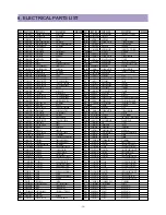
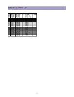
ELECTRICAL PARTS LIST
E007
4856310300
EYE LET
BSR T0.2 (R1.6)
E008
4856310300
EYE LET
BSR T0.2 (R1.6)
E009
4856310300
EYE LET
BSR T0.2 (R1.6)
E010
4856310300
EYE LET
BSR T0.2 (R1.6)
E011
4856310600
EYE LET
BSR T0.2 (R2.3)
E012
4856310600
EYE LET
BSR T0.2 (R2.3)
E013
4856310600
EYE LET
BSR T0.2 (R2.3)
E014
4856310600
EYE LET
BSR T0.2 (R2.3)
E018
4856310300
EYE LET
BSR T0.2 (R1.6)
E019
4856310300
EYE LET
BSR T0.2 (R1.6)
E020
4856310300
EYE LET
BSR T0.2 (R1.6)
E021
4856310300
EYE LET
BSR T0.2 (R1.6)
E022
4856310600
EYE LET
BSR T0.2 (R2.3)
E023
4856310600
EYE LET
BSR T0.2 (R2.3)
E024
4856310600
EYE LET
BSR T0.2 (R2.3)
E025
4856310600
EYE LET
BSR T0.2 (R2.3)
E026
4856310300
EYE LET
BSR T0.2 (R1.6)
E027
4856310300
EYE LET
BSR T0.2 (R1.6)
E028
4856310300
EYE LET
BSR T0.2 (R1.6)
E029
4856310300
EYE LET
BSR T0.2 (R1.6)
E030
4856310300
EYE LET
BSR T0.2 (R1.6)
E031
4856310600
EYE LET
BSR T0.2 (R2.3)
E032
4856310600
EYE LET
BSR T0.2 (R2.3)
E033
4856310300
EYE LET
BSR T0.2 (R1.6)
E034
4856310300
EYE LET
BSR T0.2 (R1.6)
E035
4856310300
EYE LET
BSR T0.2 (R1.6)
E036
4856310600
EYE LET
BSR T0.2 (R2.3)
E037
4856310600
EYE LET
BSR T0.2 (R2.3)
E038
4856310600
EYE LET
BSR T0.2 (R2.3)
E039
4856310600
EYE LET
BSR T0.2 (R2.3)
E040
4856310300
EYE LET
BSR T0.2 (R1.6)
E042
4856310300
EYE LET
BSR T0.2 (R1.6)
E043
4856310600
EYE LET
BSR T0.2 (R2.3)
E044
4856310600
EYE LET
BSR T0.2 (R2.3)
E045
4856310600
EYE LET
BSR T0.2 (R2.3)
E046
4856310600
EYE LET
BSR T0.2 (R2.3)
E047
4856310600
EYE LET
BSR T0.2 (R2.3)
E048
4856310300
EYE LET
BSR T0.2 (R1.6)
E049
4856310300
EYE LET
BSR T0.2 (R1.6)
E050
4856310600
EYE LET
BSR T0.2 (R2.3)
E051
4856310600
EYE LET
BSR T0.2 (R2.3)
E059
4856310600
EYE LET
BSR T0.2 (R2.3)
E060
4856310600
EYE LET
BSR T0.2 (R2.3)
E065
4856310600
EYE LET
BSR T0.2 (R2.3)
E066
4856310600
EYE LET
BSR T0.2 (R2.3)
E067
4856310600
EYE LET
BSR T0.2 (R2.3)
E068
4856310600
EYE LET
BSR T0.2 (R2.3)
E069
4856310600
EYE LET
BSR T0.2 (R2.3)
E070
4856310600
EYE LET
BSR T0.2 (R2.3)
E080
4856310600
EYE LET
BSR T0.2 (R2.3)
E081
4856310600
EYE LET
BSR T0.2 (R2.3)
N0010
4857417500
TERM PIN
DA-IB0214(D2.3/DY PIN)
N0011
4857417500
TERM PIN
DA-IB0214(D2.3/DY PIN)
N0012
4857417500
TERM PIN
DA-IB0214(D2.3/DY PIN)
N0013
4857417500
TERM PIN
DA-IB0214(D2.3/DY PIN)
N005
4857417500
TERM PIN
DA-IB0214(D2.3/DY PIN)
N006
4857417500
TERM PIN
DA-IB0214(D2.3/DY PIN)
N007
4857417500
TERM PIN
DA-IB0214(D2.3/DY PIN)
N008
4857417500
TERM PIN
DA-IB0214(D2.3/DY PIN)
P402
485923182S
CONN WAFER
YW025-05 (STICK)
P501
485923202S
CONN WAFER
YW025-07 (STICK)
P601
485923172S
CONN WAFER
YW025-04 (STICK)
P602
485923182S
CONN WAFER
YW025-05 (STICK)
P603
485923192S
CONN WAFER
YW025-06 (STICK)
P701
485923172S
CONN WAFER
YW025-04 (STICK)
PD01
485923162S
CONN WAFER
YW025-03 (STICK)
R310
RS02Z129JS
R M-OXIDE FILM
2W 1.2 OHM J SMALL
R317
RS02Z100JS
R M-OXIDE FILM
2W 10 OHM J SMALL
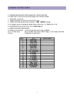
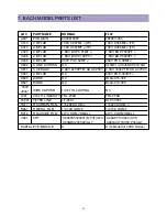
LOC
PART CODE
PART NAME
DESCRIPTION
REMARK
R403
RS01Z272J-
R M-OXIDE FILM
1W 2.7K OHM J (TAPPING)
R404
RS02Z101JS
R M-OXIDE FILM
2W 100 OHM J SMALL
R406
RS02Z203JS
R M-OXIDE FILM
2W 20K OHM J SMALL
R407
RS02Z102JS
R M-OXIDE FILM
2W 1K OHM J SMALL
R408
RF01Z100J-
R FUSIBLE
1W 10 OHM J (TAPPING)
R409
RS01Z103J-
R M-OXIDE FILM
1W 10K OHM J (TAPPING)
R414
RS02Z203JS
R M-OXIDE FILM
2W 20K OHM J SMALL
R419
RS02Z201JS
R M-OXIDE FILM
2W 200 OHM J SMALL
R422
85801060GY
WIRE COPPER
1/0.6 TIN COATING
R807
RF02Z188K-
R FUSIBLE
2W 0.18 OHM K (TAPPING)
R813
RF02Z688K-
R FUSIBLE
2W 0.68 OHM K (TAPPING)
R830
RS02Z104JS
R M-OXIDE FILM
2W 100K OHM J SMALL
ZZ200
PTMPJRE135
PCB MAIN RADIAL AS
DTU-29M5ME
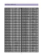
C102
CEXF1C100V
C ELECTRO
RSS 16V 10MF 4X7
C104
CEXF1H101V
C ELECTRO
50V RSS 100MF (8X11.5) TP
C106
CEXF1H101V
C ELECTRO
50V RSS 100MF (8X11.5) TP
C128
CEXF1H229V
C ELECTRO
50V RSS 2.2MF (5X11) TP
C130
CEXF1C101V
C ELECTRO
16V RSS 100MF (6.3X11) TP
C301
CMXM2A393J
C MYLAR
100V 0.039MF J (TP)
C305
CMXL1J104J
C MYLAR
63V MEU 0.1MF J
C306
CMXL1J104J
C MYLAR
63V MEU 0.1MF J
C313
CMXM2A473J
C MYLAR
100V 0.047MF J (TP)
C314
CMXM2A473J
C MYLAR
100V 0.047MF J (TP)
C402
CCXB2H222K
C CERA
500V B 2200PF K (TAPPING)
C403
CMXM2A103J
C MYLAR
100V 0.01MF J (TP)
C410
CCXB2H561K
C CERA
500V B 560PF K (TAPPING)
C411
CEXF2E229V
C ELECTRO
250V RSS 2.2MF (8X11.5)TP
C412
CCXB2H221K
C CERA
500V B 220PF K (TAPPING)
C413
CMXL1J104J
C MYLAR
63V MEU 0.1MF J
C414
CMXM2A473J
C MYLAR
100V 0.047MF J (TP)
C416
CCXB2H102K
C CERA
500V B 1000PF K (TAPPING)
C425
CCXB2H102K
C CERA
500V B 1000PF K (TAPPING)
C601
CEXF1E470V
C ELECTRO
RSS 25V 47MF 5X11 P5.0 TA
C602
CMXL1J224J
C MYLAR
63V MEU 0.22MF J (TP)
C603
CMXL1J224J
C MYLAR
63V MEU 0.22MF J (TP)
C604
CEXF1H100V
C ELECTRO
50V RSS 10MF (5X11) TP
C605
CCXB1H682K
C CERA
50V B 6800PF K (TAPPING)
C606
CCXB1H682K
C CERA
50V B 6800PF K (TAPPING)
C607
CMXM2A104J
C MYLAR
100V 0.1MF J (TP)
C608
CMXM2A104J
C MYLAR
100V 0.1MF J (TP)
C609
CMXM2A104J
C MYLAR
100V 0.1MF J (TP)
C610
CMXM2A104J
C MYLAR
100V 0.1MF J (TP)
C614
CEXF1C470V
C ELECTRO
16V RSS 47MF (5X11) TP
C701
CEXF1C101V
C ELECTRO
16V RSS 100MF (6.3X11) TP
C704
CEXF1E470V
C ELECTRO
RSS 25V 47MF 5X11 P5.0 TA
C707
CEXF1C101V
C ELECTRO
16V RSS 100MF (6.3X11) TP
C713
CEXF1C470V
C ELECTRO
16V RSS 47MF (5X11) TP
C716
CEXF1C101V
C ELECTRO
16V RSS 100MF (6.3X11) TP
C721
CEXF1C101V
C ELECTRO
16V RSS 100MF (6.3X11) TP
C722
CMXL1J224J
C MYLAR
63V MEU 0.22MF J (TP)
C723
CEXF1H229V
C ELECTRO
50V RSS 2.2MF (5X11) TP
C726
CMXL1J104J
C MYLAR
63V MEU 0.1MF J
C727
CEXF1C101V
C ELECTRO
16V RSS 100MF (6.3X11) TP
C730
CEXF1C101V
C ELECTRO
16V RSS 100MF (6.3X11) TP
C731
CEXF1E470V
C ELECTRO
RSS 25V 47MF 5X11 P5.0 TA
C732
CMXL1J224J
C MYLAR
63V MEU 0.22MF J (TP)
C734
CMXL1J224J
C MYLAR
63V MEU 0.22MF J (TP)
C735
CEXF1C101V
C ELECTRO
16V RSS 100MF (6.3X11) TP
C740
CEXF1C101V
C ELECTRO
16V RSS 100MF (6.3X11) TP
C749
CEXF1C101V
C ELECTRO
16V RSS 100MF (6.3X11) TP
C751
CMXL1J104J
C MYLAR
63V MEU 0.1MF J
C752
CMXM2A104J
C MYLAR
100V 0.1MF J (TP)
C753
CMXL1J104J
C MYLAR
63V MEU 0.1MF J
C754
CMXL1J154J
C MYLAR
63V MEU 0.15MF J
C755
CEXF1H109V
C ELECTRO
50V RSS 1MF (5X11) TP
C756
CEXF1H100V
C ELECTRO
50V RSS 10MF (5X11) TP
C758
CMXL1J224J
C MYLAR
63V MEU 0.22MF J (TP)
C759
CMXM2A682J
C MYLAR
100V 6800PF J (TP)
LOC
PART CODE
PART NAME
DESCRIPTION
REMARK
Summary of Contents for DTU-29M5ME
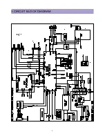
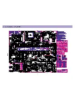
Page 5: ...4 3 CIRCUIT BLOCK DIAGRAM...
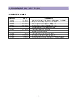
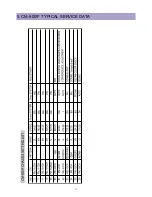
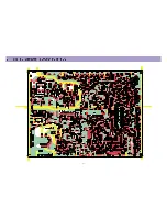
Page 16: ...15 5 CM 500 F TYPICAL SERVICE DATA...
Page 26: ...25...
Page 27: ...26...
Page 28: ...27...
Page 29: ...28...
Page 30: ...29 DTU 29M5...
Page 31: ...30 DTU 29M6...
Page 32: ...31 DTU 29M7...
Page 33: ...32 DTU 29U1...
Page 35: ...34 CM 500F 4858311110 DTU 29U8 4859645360 12W 8 SP 58126F DTU 29U8...
Page 36: ...35 DTU 29F1 CM 500F 4859845360 CPT A68AKY13X CM 500F CM 500F DTU 29F1...
Page 37: ...36 DTU 29F2 CM 500F 4859845360 CPT A68AKY13X CM 500F DTU 29F2...
Page 38: ...37 DTU 29F3 CM 500F 4859845360 CPT A68AKY13X CM 500F CM 500F DTU 29F3...
Page 40: ...39 IC DESCRIPTION...


