-58-
IC DESCRIPTION
available on one of the other CVBS inputs.In this condition the connections between the vision
IF amplifier and the synchronisation circuit can be switched on and off by means of the VDX bit.
The VDXEN bit must be set to “1” for this mode.
The vertical synchronisation is realised by means of a divider circuit.
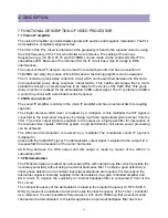
7.7 Horizontal and vertical drive
The horizontal drive is switched on and off via the soft start/stop procedure. The soft start
function is realised by means of variation of the TON of the horizontal drive pulses. During the
soft-stop period the horizontal output frequency is doubled resulting in a reduction of the EHT
so that the picture tube capacitance can easily be discharged. In addition the horizontal drive
circuit has a ‘low-power start-up’ function.
The vertical ramp generator needs an external resistor and capacitor. For the vertical drive a
differential output current is available. The outputs must be DC coupled to the vertical output
stage.
The IC has the following geometry control functions:
> Vertical amplitude
> Vertical slope
> S-correction
> Vertical shift
> Vertical zoom
> Vertical scroll
> Vertical linearity correction. When required the linearity setting for the upper and lower part of
the screen can have a different setting.
> Horizontal shift
> EW width
> EW parabola width
> EW upper and lower corner parabola correction
> EW trapezium correction
> Horizontal parallelogram and bow correction.
When the East-West geometry function is not required (e.g. for 90 picture tubes) the EW output
pin can be used for the connection of the AVL capacitor. This function is chosen by means of
the AVLE bit.
7.8 Chroma, luminance and feature processing
Some versions contain a 4H/2H(2D) adaptive PAL/NTSC comb filter. The comb filter is
automatically activated when standard CVBS signals are received.A signal is considered as
“standard signal” when a PAL or NTSC signal is identified and when the vertical divider is in the
modes ‘standard narrow window’ or ‘standard TV norm’.For non-standard signals and for
SECAM signals the comb filter is bypassed and the signal is filtered by means of bandpass and
trap filters.
The chroma band-pass and trap circuits (including the SECAM cloche filter) are realised by
means of internal filters and are tuned to the right frequency by comparing the tuning frequency
with the reference frequency of the colour decoder.
Summary of Contents for DTU-29M5ME
Page 5: ...4 3 CIRCUIT BLOCK DIAGRAM...
Page 16: ...15 5 CM 500 F TYPICAL SERVICE DATA...
Page 26: ...25...
Page 27: ...26...
Page 28: ...27...
Page 29: ...28...
Page 30: ...29 DTU 29M5...
Page 31: ...30 DTU 29M6...
Page 32: ...31 DTU 29M7...
Page 33: ...32 DTU 29U1...
Page 35: ...34 CM 500F 4858311110 DTU 29U8 4859645360 12W 8 SP 58126F DTU 29U8...
Page 36: ...35 DTU 29F1 CM 500F 4859845360 CPT A68AKY13X CM 500F CM 500F DTU 29F1...
Page 37: ...36 DTU 29F2 CM 500F 4859845360 CPT A68AKY13X CM 500F DTU 29F2...
Page 38: ...37 DTU 29F3 CM 500F 4859845360 CPT A68AKY13X CM 500F CM 500F DTU 29F3...
Page 40: ...39 IC DESCRIPTION...

