background image

29

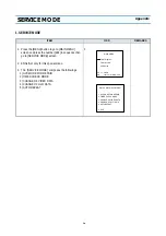
SERVICE MODE

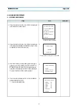
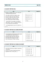
4. CHANGE OF EEPROM DATA

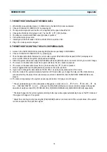
5. CHANGE OF EEPROM DATA DURING PB MODE

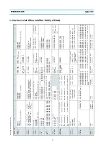
6. CHANGE OF EEPROM DATA DURING SLOW MODE

ITEM

OSD

REMARKS

* [CHANGE OF EEPROM DATA] is used to change the 

VIDEO/AUDIOcharacteristic data.

1. Press number [3] button to activate the mode.
2. Press [


¡

ç


] button to move from right to left.

3. Press [


¡

æ


] button to move from up to down.

4. Press [OK] button to toggle the bit of data.
5. Then Press [0] button to confirm the change.

* System data can be changed by pressing [PAL/
SECAM] button. Then "A" is changed as "P 

¡

æ

 M 

¡

æ


A" by turn whenever the key is pressed.

* For SECAM model, the order is "A 

¡

æ


¡

æ


¡

æ


M  

¡

æ

A".

ITEM

OSD

REMARKS

1. Press number [3] button  to activate the mode during PlayBack.

* Press [REC] button to adjust PG (6.5H)

2. Press [


¡

ç


] button to move from right to left.

3. Press [


¡

æ


] button to move from up to down.

4. Press [OK] button to toggle the bit of data.
5. Then Press [0] button to confirm the change.

ITEM

OSD

REMARKS

1. Press number [3] button to activate the mode during 

SLOW mode.

2. Press [


¡

ç


/


¡

æ


] button to adjust SLOW tracking.

3. Adjustment steps : [0 - 99]  & [-99 - 0]

0  0  0  1  1  1  0  1    A1

1  1  1  1  1  1  1  0    A2
1  0  0  0  0  0  1  0   A3

1  0  1  0  0  0  1  0    A4
1  1  0  1  1  0  1  1    A5

0  1  0  0  1  0  1  0    A6
0  1  0  0  0  1  0  0    A7

0  0  1  1  0  0  1  0    A8

0 RETURN

0  0  0  1  1  1  0  1    A1
1  1  1  1  1  1  1  0    A2

1  0  0  0  0  0  1  0   A3
1  0  1  0  0  0  1  0    A4

1  1  0  1  1  0  1  1    A5
0  1  0  0  1  0  1  0    A6

0  1  0  0  0  1  0  0    A7
0  0  1  1  0  0  1  0    A8

0 RETURN    REC PG (6.5H)

0  0  0  1  1  1  0  1    A1
1  1  1  1  1  1  1  0    A2

1  0  0  0  0  0  1  0   A3
1  0  1  0  0  0  1  0    A4

1  1  0  1  1  0  1  1    A5
0  1  0  0  1  0  1  0    A6

0  1  0  0  0  1  0  0    A7
0  0  1  1  0  0  1  0    A8

0 RETURN     -/

Z

 SLOW  00

Appendix

Summary of Contents for DV- K213S Series

Page 1: ...ssette Recorder Model SECAM MODELS DV K813S K413S K213S Series DV K823S K423S K223S Series DV K843S K443S K243S Series DV K863S K463S K263S Series DV K873S K473S K273S Series DV K893S K493S K293S Seri...

Page 2: ...UIT DIAGRAM 18 SW CIRCUIT DIAGRAM 19 SHUTTLE PATH JIG DIAGRAM 20 WAVEFORMS ON VIDEO CIRCUIT 21 COMPONENTS LOCATION GUIDE ON PCB BOTTOM VIEW 24 PCB MAIN 24 DISASSEMBLY 25 PACKING ASS Y 24 FRONT PANEL A...

Page 3: ...ielectric strengthen between power cord plug prongs and exposed accessible parts of the set RF terminals antenna terminals video and audio input output terminals microphone jack ear phone jacks etc is...

Page 4: ...rts Use on AC voltmeter to measure across both terminals of load Z See figure2 and following table Leakage current ratings for selected are as AC Line Voltage Region Load Z Leakage Current i Clearance...

Page 5: ...4 1 FRONT VIEWS FUNCTION DV K813S FRONT VIEW DV K823S FRONT VIEW DV K833S FRONT VIEW DV K843S FRONT VIEW EXTERNAL VIEWS...

Page 6: ...K863S FRONT VIEW DV K873S FRONT VIEW DV K893S FRONT VIEW DV K9A3S FRONT VIEW POWER REWIND REVIEW STOP EJECT FAST FORWARD CUE RECORD PLAY BACK FRONT VIDEO AUDIO INPUT JACK CHANNEL UP DOWN L R EXTERNAL...

Page 7: ...6 EXTERNAL VIEWS 2 REAR VIEWS FUNCTION MONO 2 SCART TYPE REAR VIEW HI FI 2 SCART TYPE REAR VIEW...

Page 8: ...Insert PATH JIG and press REC button on the remote control 5 Check the position of the V sync from the rising edge of the SW pulse Standard 6 5H 0 5H ITEM MODE ADJUSTMENT POINT CHECK POINT TEST EQUIP...

Page 9: ...anced 45dB Rhode Schwarz noise meter with NETTETE IMAGE control at cen ter position 240 lines with NETTETE IMAGE control at center position AUDIO Recording system Input Output Frequency Range Signal t...

Page 10: ...3 ATM24C16 PIN NO REC PB 1 0 0 2 0 0 3 0 0 4 0 0 5 3 9 3 9 6 3 9 4 7 0 0 8 5 24 5 29 MOTOR DRIVE IC IC502 KA3082 PIN NO REC PB 1 0 0 2 0 55 0 55 3 8 78 0 88 4 6 24 6 24 5 0 01 0 01 6 0 01 0 01 7 12 12...

Page 11: ...5 87 2 3 2 1 13 2 1 1 6 38 5 5 63 5 5 88 2 3 2 1 14 2 1 1 6 39 2 7 2 7 64 4 25 4 25 89 2 3 2 1 15 2 3 2 3 40 5 5 65 2 1 2 3 90 5 5 16 0 0 7 41 5 5 66 5 5 91 2 3 2 1 17 2 5 1 8 42 1 7 1 7 67 5 5 92 2...

Page 12: ...3 79 43 3 95 4 11 3 81 3 81 22 3 81 3 81 33 3 86 3 77 44 1 74 2 1 NICAM IC IC051 MSP3417DQ PIN NO EE PIN NO EE 1 0 03 27 0 2 2 29 28 0 3 0 01 29 0 4 0 01 30 3 69 5 0 31 3 7 6 4 95 32 0 7 3 95 33 8 25...

Page 13: ...9 0 20 0 23 0 03 3 3 7 3 7 9 0 0 15 0 0 21 2 43 0 4 4 85 4 9 10 0 0 16 31 9 31 9 22 2 01 0 01 5 4 3 9 11 3 9 4 17 0 0 23 2 69 0 6 0 0 12 3 7 3 7 18 0 0 24 2 74 0 24 1 66 50 0 25 1 69 51 2 32 26 0 52...

Page 14: ...OMPO NET VALUES WHICH HAVE TO BE MODIFIED ACCORD ING TO THE APPLIED VIDEO IC LOC C210 R 2 2uF 50V 10uF 16V 2 2uF 50V C305 C 39pF 56pF 56pF C415 R 10uF 16V 2 2uF 50V 10uF 16V L302 A 82uH 150uH 150uH RA...

Page 15: ...14 CIRCUIT DIAGRAM 1 POWER CIRCUIT DIAGRAM 230V ONLY...

Page 16: ...15 CIRCUIT DIAGRAM 2 SYSCON CIRCUIT DIAGRAM...

Page 17: ...16 CIRCUIT DIAGRAM 3 A V CIRCUIT DIAGRAM SECAM...

Page 18: ...17 4 PIF CIRCUIT DIAGRAM CIRCUIT DIAGRAM...

Page 19: ...18 CIRCUIT DIAGRAM 5 HIFI SW CIRCUIT DIAGRAM...

Page 20: ...19 CIRCUIT DIAGRAM 6 SW CIRCUIT DIAGRAM...

Page 21: ...501 D502 D503 D504 D507 D509 D512 D513 D514 PAL B G BG DK PAL I I I SECAM PAL B G BG DK PAL I I I SECAM SECAM FRANCE X X SECAM SWISS X O NON PDC X X PDC1 X O PDC2 O X PDC3 O O 1 MIN X 30 MIN O NOT APP...

Page 22: ...301 300mVp p Pin 61 of IC301 400mVp p Pin 28 of IC301 C SYNC 2Vp p 9 10 11 1 Pin 36 of IC301 SECAM color bar input 1 0Vp p 2 Pin 36 of IC301 PAL color bar input 1 0Vp p 3 Pin 29 of IC301 SECAM color b...

Page 23: ...E LUMINANCE IN THE PB MODE DP 1 TEST TAPE Pin 16 of IC361 SECAM color input 1 0Vp p Pin 12 of IC361 200mVp p Pin 28 of IC301 C SYNC 2Vp p 12 14 13 UP Pin 11 of IC301 color rotary 1Vp p DOWN Pin 74 of...

Page 24: ...Pin 11 of IC301 color rotary 0 5Vp p DOWN Pin 74 of IC301 500mVp p Pin 29 of IC301 Video out 2 0Vp p Pin 57 59 of IC301 240mVp p Pin 61 of IC301 300mVp p 19 20 21 22 UP Pin 11 of IC301 color rotary 0...

Page 25: ...24 COMPONENTS LOCATION GUIDE ON PCB BOTTOM VIEW 1 PCB MAIN...

Page 26: ...25 DISASSEMBLY 1 PACKING ASS Y...

Page 27: ...26 DISASSEMBLY 2 FRONT PANEL ASSEMBLY DV K813S SERIES DV K823S SERIES...

Page 28: ...27 DISASSEMBLY DV K873S SERIES DV K893S SERIES...

Page 29: ...28 DISASSEMBLY DV K843S SERIES DV K863S SERIES...

Page 30: ...29 DISASSEMBLY DV K9A3S SERIES...

Page 31: ...30 DISASSEMBLY 3 INSTRUMENT DISASSEMBLY 3 1 TOP COVER REMOVAL FIG 1 1 Remove five 5 screws holding the top cover 2 Carefully lift the back of the top cover and slide to the rear to remove...

Page 32: ...31 DISASSEMBLY 3 2 FRONT PANEL REMOVAL FIG 2 1 Remove the top cover 2 Release seven 7 tabs holding the front panel 3 Remove the front panel...

Page 33: ...32 DISASSEMBLY 3 3 BOTTOM COVER REMOVAL FIG 3 1 Remove the top cover and front panel 2 Remove three 3 screws 3 Release four 4 tabs and lift out the bottom cover...

Page 34: ...33 DISASSEMBLY 3 4 F L DOOR REMOVAL FIG 4 1 Open the F L door 90 2 Remove the F L door in the direction of arrow...

Page 35: ...34 DISASSEMBLY 3 5 COVER PRE AMP DECK AS REMOVAL FIG 5 1 Remove five 5 screws 2 Disconnect the connector and FPC 3 Pull out the DECK AS and COVER PRE AMP in the direction of arrow...

Page 36: ...35 DISASSEMBLY 3 6 PCB MAIN AS REMOVAL FIG 6 1 Remove two 2 screws 2 Release three 3 tabs and lift out the main PCB in the direction of arrow...

Page 37: ...RKT TOT AS K MECHA 2 B1910 97S8103600 L C MOTOR MDH2B70 B1940 5SSF1DKM10 SW CAM MMS00320ZMBO A1901 7274300611 SCREW TAPPTITE TT3 RND 3X6 MFZN A2100 97SA311600 IDLER PLATE AS K MECHA A2200 97S3108200 P...

Page 38: ...Y5V 0 1MF Z 2012 C216 HCBK102KCA C CHIP CERA 50V X7R 1000PF K 2012 C239 HCLK331JCA C CHIP CERA 50V SL 330PF J 2012 C251 HCFH474ZCA C CHIP CERA 25V Y5V 0 47MF Z 2012 C252 HCFH474ZCA C CHIP CERA 25V Y5V...

Page 39: ...J 2012 C627 HCBK103KCA C CHIP CERA 50V X7R 0 01MF K 2012 C628 HCBK223KCA C CHIP CERA 50V X7R 0 022MF K 2012 C630 HCBK103KCA C CHIP CERA 50V X7R 0 01MF K 2012 C631 HCBK103KCA C CHIP CERA 50V X7R 0 01MF...

Page 40: ...ODE PART NAME PART DISC REMARK R227 HRFT229JCA R CHIP 1 10 2 2 OHM J 2012 R228 HRFT229JCA R CHIP 1 10 2 2 OHM J 2012 R229 HRFT103JCA R CHIP 1 10 10K OHM J 2012 R230 HRFT512JCA R CHIP 1 10 5 1K OHM J 2...

Page 41: ...332K C CERA 50V B 3300PF K TAPPING LOC PART CODE PART NAME PART DISC REMARK C018 CCXB1H332K C CERA 50V B 3300PF K TAPPING C055 CEXF1C100A C ELECTRO 16V RSM 10MF 4X7 C057 CEXF1C100A C ELECTRO 16V RSM 1...

Page 42: ...6 3X11 TP C809 CMXL2G333K C MYLAR 400V MEU 0 033MF K C824 CEXK1J220L C ELECTRO 63V 22UF KXL C826 CEXF1H100A C ELECTRO 50V RSM 10MF 5X7 TP LOC PART CODE PART NAME PART DISC REMARK C828 CEXF1E221V C ELE...

Page 43: ...50V HIKF 0 1MF Z LOC PART CODE PART NAME PART DISC REMARK C302 CCZF1H473Z C CERA 50V F 0 047MF Z C323 CCZF1H104Z C CERA 50V HIKF 0 1MF Z C325 CCZF1H104Z C CERA 50V HIKF 0 1MF Z C329 CCZF1H104Z C CERA...

Page 44: ...060TA WIRE COPPER 0 6X52MM TAPING LOC PART CODE PART NAME PART DISC REMARK JP038 85801060TA WIRE COPPER 0 6X52MM TAPING JP039 85801060TA WIRE COPPER 0 6X52MM TAPING JP041 85801060TA WIRE COPPER 0 6X52...

Page 45: ...47K OHM J R404 RD AZ473J R CARBON FILM 1 6 47K OHM J LOC PART CODE PART NAME PART DISC REMARK R405 RD AZ511J R CARBON FILM 1 6 510 OHM J R406 RD AZ511J R CARBON FILM 1 6 510 OHM J R5A1 RD AZ333J R CAR...

Page 46: ...1 6 68 OHM J R824 RD AZ470G R CARBON FILM 1 6 47 OHM G R825 RD AZ132G R CARBON FILM 1 6 1 3K OHM G R827 RD AZ241J R CARBON FILM 1 6 240 OHM J R830 RD 2Z301JS R CARBON FILM 1 2 300 OHM J SMALL R832 RD...

Page 47: ...6 85801065GY WIRE COPPER AWG22 1 0 65 TIN COATING LOC PART CODE PART NAME PART DISC REMARK JP147 85801065GY WIRE COPPER AWG22 1 0 65 TIN COATING JP148 85801065GY WIRE COPPER AWG22 1 0 65 TIN COATING J...

Page 48: ...9 85801065GY WIRE COPPER AWG22 1 0 65 TIN COATING LOC PART CODE PART NAME PART DISC REMARK JP240 85801065GY WIRE COPPER AWG22 1 0 65 TIN COATING JP241 85801065GY WIRE COPPER AWG22 1 0 65 TIN COATING J...

Page 49: ...DAEWOO ELECTRONICS CO LTD 686 AHYEON DONG MAPO GU SEOUL KOREA C P O BOX 8003 SEOUL KOREA TELEX DWELEC K28177 8 CABLE DAEWOOELEC E mail leesk web dwe co kr TEL 82 2 360 7802 FAX 82 2 360 7877...

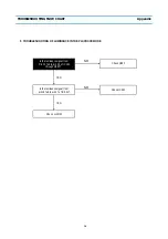
Page 50: ...y GND however it is not necessary to isolate the oscilloscope when check the secondary circuit A CHECKING THE PRIMARY CIRCUIT No output Voltage NO NO NO YES Prepare the oscilloscope connected the isol...

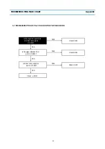
Page 51: ...OUBLESHOOTING FLOW CHART B CHECKING THE SECONDARY CIRCUIT Check each output voltage Check trans former Check any diode which causes no power Check any COIL or capacitor which causes no power END Appen...

Page 52: ...o Out point Pin No 21 of TMI Block Check the A V Switching and Video Circduit In case of 2 SCART System Check the Power Supply Circuit NO Check Q001 Q002 Q003 D003 and Power Supply Circuit Check the S...

Page 53: ...k YES NO NO NO YES YES Adjust tracking Noise appears although change cassette tape YES Is CTL pulse output at pin 97 of IC501 Playback picture is not good YES NO Check IC501 The voltage of pin 7 of IC...

Page 54: ...on the whole Noise appears on the screen at the bottom Change Drum Ass y Is Enve waveform supplied to pin 5 of P504 Check connector and Head dust NO NO YES Check pattern Check video circuit Adjust the...

Page 55: ...TING FLOW CHART C Auto stop during playback NO Is reel pulse applied to pin 79 and 80 of IC501 Check reel sensor NO YES Is D FG applied to pin 89 of IC501 YES Check IC501 Check connector and D FG circ...

Page 56: ...OOTING FLOW CHART D Drum M T loading stops NO NO Is motor 12V supplied from IC502 pin7 8 Check Q503 Check power module NO YES YES Is 5 2V supplied from POWER CIRCUIT Check D519 Check connector and mot...

Page 57: ...or Capstan M T loading stops NO YES Is motor 17V supplied Check power Module NO Is the input of pin 6 of P501 2 5V 3 5V Check circuit of R583 R582 C550 YES NO Is pin 4 of P501 2 5V Check R581 R579 YES...

Page 58: ...pplied to pin 58 of IC501 Check C sync of video IC and pattern Check motor YES Emergency mode when plugging power cord NO YES Is ever 5V applied Check power Module NO Does X501 crystal oscillate Check...

Page 59: ...Cassette is not inserted NO YES YES YES NO Is motor 13V supplied Check power Module NO NO CAM DATA is changed when CST IN Check connector Check IC501 Check Deck part Is 5V supplied at pin 81 of IC501...

Page 60: ...on does not operate NO YES YES YES When mains is unplugged is 3 6V at pin 37 of IC501 Check C524 C525 C526 NO Is sine signal applied to pin 35 and 36 of IC501 Check X502 NO Is 5V at pin 34 of IC501 Ch...

Page 61: ...de Is the output at pin 96 of IC301 Check power circuit YES YES YES YES YES YES NO NO NO NO Is 5V applied to IC301 Check A V select circuit IS collector of Q204 GND Check Q204 Q205 Q206 Check pattern...

Page 62: ...ct circuit YES NO Is the voltage above 4V at REC H Is clock and data applied to pin 23 24 of IC301 NO Check SYSCON YES NO Is signal input into pin 1 of IC301 Check R201 R202 C203 NO Change IC301 YES Y...

Page 63: ...k IC501 NO NO YES Playback picture is not good YES Is there output at pin 76 or 78 of IC301 YES NO YES Check SCART jack YES Is there output at pin 96 of IC301 Check pattern NO Is 5V applied to Ic301 C...

Page 64: ...OFF 5V supplied to IC301 at 5 volts YES Is the CLK DATA signal obtained from pin 23 24 of IC301 YES YES Is the signal from pin 36 of IC301 fed to pin 29 of IC301 YES Is the video signal obtained from...

Page 65: ...eck drum and deck mechanism NO Check H A SW NO Is REC H from pin 75 of Ic501 Is H A SW from pin 18 of IC501 Check REC H YES NO Is video SW from pin 18 of IC501 supplied to pin 11 of IC301 Check video...

Page 66: ...l from pin 21 of IC601 fed to pin 36 of IC301 Is ON OFF 5V supplied to IC301 at 5 volts YES YES Check PCB pattern and adjacent circuits Check ON OFF 5V Check IC301 Check Q302 C311 R311 and R312 NO Che...

Page 67: ...in 21 of IC601 fed to pin 36 of IC301 Check AV SW circuit Check PCB pattern and adjacent circuit NO Check ON OFF 5V NO Check IC301 NO Check C349 C350 YES YES YES YES YES Is ON OFF 5V supplied to IC301...

Page 68: ...of IC361 through pin 30 of IC301 NO Check IC361 NO Check ON OFF 5V NO Check IC 361 NO Check Q361 Q365 D361 YES YES YES YES Is ON OFF 5V supplied to pin 5 and pin 17 of IC 361 at 5 volts Is the signal...

Page 69: ...LESHOOTING OF LUMINANCE IN THE PLAYBACK MODE NO Check Q302 NO Check IC 301 YES Is the luminance signal from Pin 21 fed to pin 20 of IC 301 through Q302 Is the luminance signal from pin 18 fed to pin 1...

Page 70: ...OLOUR IN THE PLAYBACK MODE NO Check IC301 NO Check IC301 NO Check C ROT YES Is the signal from pin 52 54 of IC 301 fed to pin 51 of IC 301 Is the signal obtained from pin 61 of IC301 Is colour rotary...

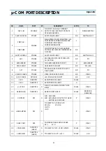
Page 71: ...P72 AN2 I USE FOR PATH ADJUST A D PATH JIG 8 AFT P71 AN1 I AFT ANALOG DATA INPUT FOR AUTO FINE TUNING A D PIF 9 VIDEO DC ENVE P70 AN0 I VIDEO DC ENVE DATA INPUT A D VIDEO 10 Hi Fi DC ENVE P67 AN10 I H...

Page 72: ...SET RESET I RESET INPUT L RESET IC 35 Xcin P31 I 32 768KHz OSC IN 36 Xcout P30 O 32 768KHz OSC OUT 37 Vcc Vcc BACK UP 5V 38 Xin Xin I 16MHz OSC IN 39 Xout Xout O 162MHZ OSC OUT 40 Vss Vss GND 41 OSCin...

Page 73: ...K CAM 71 II C CLK P101 SCL O A V SECAM CLK SERIAL VIDEO 72 II C DATA P100 SDA I O A V SECAM DATA SERIAL VIDEO 73 POWER ON H P97 O POWER ON OFF CONTROL PORT H POWER 74 POWER OFF H P96 O POWER ON OFF CO...

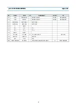
Page 74: ...Vrefout 92 AMP Vrefin AMP Vrefin AMP Vrefin 93 C P80 C 94 CTL CTL CTL 95 CTL CTL CTL 96 AMP C AMP C 97 CTL AMP CTL AMP O CTL AMP OUTPUT PATH JIG 98 AMP Vcc AMP Vcc AMP Vcc 99 Avcc Avcc Avcc 100 START...

Page 75: ...P72 AN2 I USE FOR PATH ADJUST A D PATH JIG 8 AFT P71 AN1 I AFT ANALOG DATA INPUT FOR AUTO FINE TUNING A D PIF 9 VIDEO DC ENVE P70 AN0 I VIDEO DC ENVE DATA INPUT A D VIDEO 10 Hi Fi DC ENVE P67 AN10 I H...

Page 76: ...SET RESET I RESET INPUT L RESET IC 35 Xcin P31 I 32 768KHz OSC IN 36 Xcout P30 O 32 768KHz OSC OUT 37 Vcc Vcc BACK UP 5V 38 Xin Xin I 16MHz OSC IN 39 Xout Xout O 162MHZ OSC OUT 40 Vss Vss GND 41 OSCin...

Page 77: ...K CAM 71 II C CLK P101 SCL O A V SECAM CLK SERIAL VIDEO 72 II C DATA P100 SDA I O A V SECAM DATA SERIAL VIDEO 73 POWER ON H P97 O POWER ON OFF CONTROL PORT H POWER 74 POWER OFF H P96 O POWER ON OFF CO...

Page 78: ...Vrefout 92 AMP Vrefin AMP Vrefin AMP Vrefin 93 C P80 C 94 CTL CTL CTL 95 CTL CTL CTL 96 AMP C AMP C 97 CTL AMP CTL AMP O CTL AMP OUTPUT PATH JIG 98 AMP Vcc AMP Vcc AMP Vcc 99 Avcc Avcc Avcc 100 START...

Page 79: ...for this special menu 3 The SERVICE MODE composes the followings 1 SVC MODE FOR REPAIR 2 TIMER CHECK MODE 3 CHANGE OF VIDEO DATA 4 CHANGE OF Hi Fi DATA 5 AUTO REPEAT 1 Timer Program Timer Review VCR S...

Page 80: ...REV STOP operations are executed automatically and OSD 4 will be displayed To press 0 button on OSD 4 will be ejected 4 The error state is displayed OK or NG in ERROR CHECK RESULTS screen means unchec...

Page 81: ...set to OFF mode ITEM OSD REMARKS TIMER CHECK MODE is used to check the TIMER RECORD SHOWVIEW RECORD and VFD SEG MENT 1 Press the number 2 button then OSD 1 will be dis played in the initial SVC mode...

Page 82: ...s REC button to adjust PG 6 5H 2 Press button to move from right to left 3 Press button to move from up to down 4 Press OK button to toggle the bit of data 5 Then Press 0 button to confirm the change...

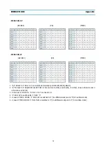
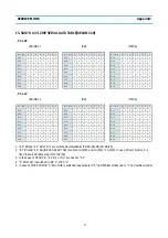
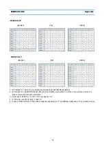
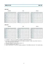
Page 83: ...moves from right to left when the button is pressed 6 The cursor on the data table moves from up to down when the button is pressed 7 Data is toggled whenever the OK button is pressed on the cursor po...

Page 84: ...CTL 4dB 010 PIC CTL 2dB 011 PIC CTL 0dB 100 PIC CTL 0dB 101 PIC CTL 2dB 110 PIC CTL 4dB 111 PIC CTL 6dB SHARP 0 APC LOOP BEFORE 1 APC LOOP AFTER 0 NORMAL PB 1 TRICK PB 0 PHASE ALTERNATION ON 1 PHASE A...

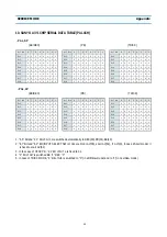
Page 85: ...0 0 1 0 1 0 Gr 4 0 1 0 1 1 0 0 1 Gr 4 0 1 0 1 1 0 0 1 Gr 4 0 1 0 1 1 0 1 0 Gr 5 1 0 0 0 0 1 0 1 Gr 5 0 1 0 0 0 1 1 0 Gr 5 0 1 0 0 0 1 0 1 Gr 6 0 0 1 1 0 0 0 1 Gr 6 1 0 1 0 0 1 0 0 Gr 6 1 0 0 0 0 1 0...

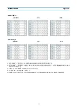
Page 86: ...0 0 0 0 1 0 1 1 Gr 4 0 1 0 1 1 0 0 1 Gr 4 0 1 0 1 1 0 0 1 Gr 4 0 1 0 1 1 0 1 0 Gr 5 1 0 0 0 0 1 0 1 Gr 5 0 1 0 0 0 1 1 0 Gr 5 0 1 0 1 0 1 0 1 Gr 6 0 0 1 1 0 0 0 1 Gr 6 1 0 1 0 0 1 0 0 Gr 6 1 0 0 0 0...

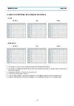
Page 87: ...1 0 1 Gr 2 0 0 0 0 1 1 0 1 Gr 3 0 0 0 0 1 0 1 0 Gr 3 0 0 0 0 1 0 1 0 Gr 3 0 0 0 0 1 0 1 0 Gr 4 0 1 0 1 1 0 0 1 Gr 4 1 0 0 1 1 0 1 0 Gr 4 1 0 0 1 1 0 1 1 Gr 5 1 0 0 0 0 1 0 1 Gr 5 0 1 0 0 0 1 1 0 Gr 5...

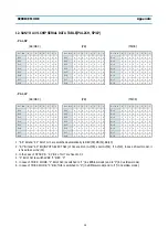
Page 88: ...0 1 Gr 2 0 0 0 0 1 1 0 1 Gr 3 0 0 0 0 1 0 1 0 Gr 3 0 0 0 0 1 0 1 0 Gr 3 0 0 0 0 1 0 1 0 Gr 4 0 1 0 1 1 0 0 1 Gr 4 0 1 0 1 1 0 0 1 Gr 4 0 1 0 1 1 0 1 0 Gr 5 1 0 0 0 0 1 0 1 Gr 5 0 1 0 0 0 1 1 0 Gr 5 0...

Page 89: ...1 Gr 3 0 0 0 0 1 0 1 1 Gr 3 0 0 0 0 1 0 1 1 Gr 3 0 0 0 0 1 0 1 1 Gr 4 0 1 0 1 1 0 0 1 Gr 4 0 1 0 1 1 0 0 1 Gr 4 0 1 0 1 1 0 1 0 Gr 5 1 0 0 0 0 1 0 1 Gr 5 0 1 0 0 0 1 1 0 Gr 5 0 1 0 1 0 1 0 1 Gr 6 0 1...

Page 90: ...1 0 0 1 Gr 4 0 1 0 1 1 0 0 1 Gr 4 0 1 0 1 1 0 0 1 Gr 5 1 0 0 0 0 1 0 1 Gr 5 0 1 0 0 0 1 1 0 Gr 5 0 1 0 0 0 1 0 1 Gr 6 0 0 1 1 0 0 1 0 Gr 6 1 0 1 0 0 1 0 0 Gr 6 1 0 0 0 0 1 0 0 Gr 7 0 0 1 1 0 1 1 0 Gr...

Page 91: ...1 1 0 0 1 Gr 4 0 1 0 1 1 0 0 1 Gr 5 1 0 0 0 0 1 0 1 Gr 5 0 1 0 0 0 1 1 0 Gr 5 0 1 0 0 0 1 0 1 Gr 6 0 0 1 1 0 0 1 0 Gr 6 1 0 1 0 0 1 0 0 Gr 6 1 0 0 0 0 1 0 0 Gr 7 0 0 1 1 0 1 1 0 Gr 7 0 0 1 1 0 1 0 0 G...

Page 92: ...1 0 0 1 Gr 4 0 1 0 1 1 0 0 1 Gr 5 1 0 0 0 1 0 0 1 Gr 5 0 1 0 0 1 0 1 0 Gr 5 0 1 0 0 1 0 0 1 Gr 6 0 0 1 1 0 0 1 0 Gr 6 1 0 1 0 0 1 0 0 Gr 6 1 0 0 0 0 1 0 0 Gr 7 0 0 1 1 0 1 1 0 Gr 7 0 0 1 1 0 1 0 0 Gr...

Page 93: ...0 1 0 0 0 0 Gr 8 0 0 0 1 0 0 0 0 Gr 8 0 0 0 1 0 0 0 0 Gr 9 0 1 1 0 0 1 0 0 Gr 9 1 1 1 0 0 1 0 0 Gr 9 1 1 1 0 0 1 0 0 Gr Bit 8 7 6 5 4 3 2 1 Gr Bit 8 7 6 5 4 3 2 1 Gr Bit 8 7 6 5 4 3 2 1 Gr 1 0 1 1 0...

Reviews: