8
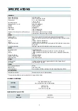
SPECIFICATIONS
CHANNEL COVERAGE
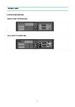
INPUT/OUTPUT JACK TYPE
GENERAL
Power Requirement
Power Consumption
Temperature
Operating position
Dimensions (W x H x D)
Weight
Format
Tape Width
Tape Speed
Maximum Recording Time with full-size cas-
sette
AC 230V, 50Hz
Max. 17W (in REC mode)
5
×
C ~ 35
×
C (Operating)
-20
×
C ~ 60
×
C
Horizontal only
360 x 90 x 288 (mm)
Approx. 3.85 Kg
VHS standard
12.65mm
(SP) : 23.39mm/sec
(LP) : 11.70mm/sec
(SP) :240min, with E-240 video cassette
(LP) :480min, with E-240 video cassette
VIDEO
Signal system
Recording system
Input
Output
Signal-to-Noise ratio
Horizontal resolution
PAL colour and CCIR monochrome signals, 625 lines/50 fields
Rotary two-head helical scan with a slant double-azimuth combination video
head
1.0Vp-p, 75ohms, unbalanced
1.0Vp-p, 75ohms, unbalanced
45dB (Rhode & Schwarz noise meter) with NETTETE IMAGE control at cen-
ter position
240 lines with NETTETE IMAGE control at center position
AUDIO
Recording system
Input
Output
Frequency Range
Signal to Noise Ratio
Audio Distortion
Longitudinal track
-8dBm, (CENELEC standard),more than 47 k-ohms, unbalanced
-6dBm, (CENELEC standard), less than 1k-ohms, unbalanced(100k-ohms,
load)
100Hz to 8,000Hz
More than 38dB
Less than 3% (SP)
TUNER
Tuning system
RF Output
Voltage synthesized tuner Programmable V/S 99CH (Hyper band)
UHF channel 21~69 (52)
TIMER
Memory programmable
Back up time
Clock exactness
99 CH
Less than 1 Min.
In accordance with the exactness of power supply frequency (50Hz)
ACCESSORIES
Provided Accessories
Remote control unit, RF Cable, Battery
SYSTEM
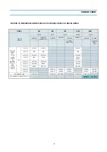
PAL, SECAM-B/G, PAL-I/I
PAL, SECAM-B/G, D/K, HYPER BAND
CHANNEL
VHF Ch 2~12
UHF Ch 21~69
CATV Ch X,Y,Z S1~S41
Model
EUROPE
Jack Type
SCART Type
*
Design and specification can be subjected to change without notice.
Summary of Contents for DV- K213S Series
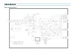
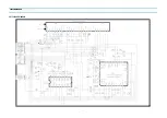
Page 15: ...14 CIRCUIT DIAGRAM 1 POWER CIRCUIT DIAGRAM 230V ONLY...
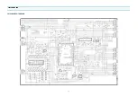
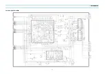
Page 16: ...15 CIRCUIT DIAGRAM 2 SYSCON CIRCUIT DIAGRAM...
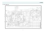
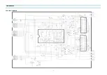
Page 17: ...16 CIRCUIT DIAGRAM 3 A V CIRCUIT DIAGRAM SECAM...
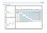
Page 18: ...17 4 PIF CIRCUIT DIAGRAM CIRCUIT DIAGRAM...
Page 19: ...18 CIRCUIT DIAGRAM 5 HIFI SW CIRCUIT DIAGRAM...
Page 20: ...19 CIRCUIT DIAGRAM 6 SW CIRCUIT DIAGRAM...
Page 25: ...24 COMPONENTS LOCATION GUIDE ON PCB BOTTOM VIEW 1 PCB MAIN...
Page 26: ...25 DISASSEMBLY 1 PACKING ASS Y...
Page 27: ...26 DISASSEMBLY 2 FRONT PANEL ASSEMBLY DV K813S SERIES DV K823S SERIES...
Page 28: ...27 DISASSEMBLY DV K873S SERIES DV K893S SERIES...
Page 29: ...28 DISASSEMBLY DV K843S SERIES DV K863S SERIES...
Page 30: ...29 DISASSEMBLY DV K9A3S SERIES...


