21
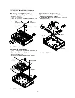
Cam Gear, and F/L Rack Removal
(Fig. 22)
1. Remove the cam gear
&
from the deck mechanism.
2. Remove the relay lever
^
from the main base
%
.
3. Remove the F/L rack
*
from the deck mechanism.
NOTE:
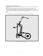
When reassembling, align the assembly as shown in
Fig. 23 & 24.
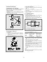
S/T Main & Sub Brakes Removal
(Fig. 25)
1. Unhook the main brake spring
!
from the T main brake
lever
#
.
2. Disconnect the main brake lever assembly
@
and T main
brake lever
#
from the main base
*
.
3. Unhook the s sub brake spring
$
from the main base and discon-
nect the s sub brake lever assembly
%
from the main base
*
.
4. Unhook the T sub brake spring
^
from the main base and discon-
nect the T sub brake lever assembly
&
from the main base
*
.
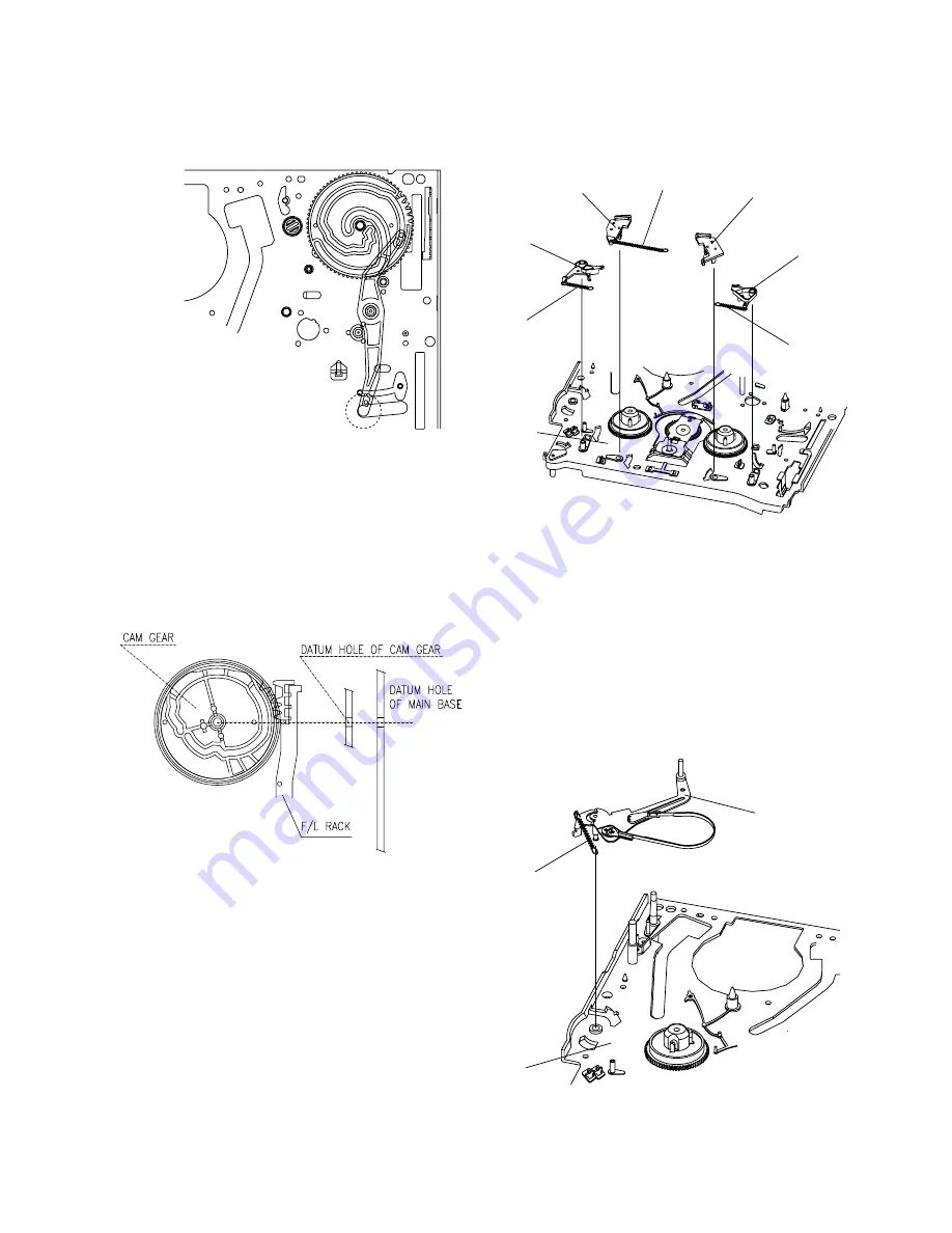
Tension Band Assembly Removal
(Fig. 26, 27)
1. Remove the tension spring
@
from the main base
!
(Fig. 26).
2. Turn the deck mechanism upside down (Fig, 27).
is facing down (Fig. 27).
3. Release the tab of the hook "A" and separate the tention band
assembly (3) (Fig. 27).
NOTE:
• After reassembling, adjust the position of the tension pole as
shown in Fig. 28.
• Avoid getting grease or oil on the felt section of the band
brake.
MECHANICAL DISASSEMBLY (Continued)
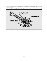
Fig. 23- L/C Bracket Assembly Alignment
Fig. 24- Cam Gear/F/L Rack Alignment
@
!
#
&
^
%
$
*
Fig. 25- Main Plate Removal
@
#
!
Fig. 26- Tension Band Assembly Removal (I)
Summary of Contents for DV- K504N-SJ
Page 35: ...34 AC001 K584NZ SJ M K584NZ SG M only...
Page 36: ...35...
Page 37: ...36...
Page 38: ...37...
Page 39: ...38...
Page 60: ...59 ELECTRICAL ADJUSTMENTS Fig 1 Circuit Board Location...
Page 92: ...91 INTERCONNECT WIRING DIAGRAM K584N K484N K384N K284N...
Page 93: ...92 POWER SUPPLY SCHEMATIC DIAGRAM FREE VOLTAGE K584NY SJ M K584NZ SJ M K584NZ SG M...
Page 95: ...94 2HD HEAD AMP SCHEMATIC DIAGRAM K384N K284N K304N...
Page 96: ...95 4HD HEAD AMP SCHEMATIC DIAGRAM K584N K484N K504N...
Page 97: ...96 VIDEO AUDIO SCHEMATIC DIAGRAM K584N K484N K384N K284N K504N K304N...
Page 98: ...97 PIF INPUT SELECTOR SCHEMATIC DIAGRAM 9V USE K584NY SJ M K584NZ SJ M K584NZ SG M...
Page 100: ...99 TIMER SYSCON SCHEMATIC DIAGRAM K584N K484N K384N K284N K504N K304N...
Page 101: ...100 POWER SUPPLY BLOCK DIAGRAM FREE VOLTAGE K584NY SJ M K584NZ SJ M K584NZ SG M...
Page 103: ...102 2HD HEAD AMP BLOCK DIAGRAM K384N K284N K304N...
Page 104: ...103 4HD HEAD AMP BLOCK DIAGRAM K584N K484N K504N...
Page 105: ...104 VIDEO AUDIO BLOCK DIAGRAM K584N K484N K384N K284N K504N K304N...
Page 106: ...105 PIF INPUT SELECTOR BLOCK DIAGRAM K584N K484N K384N K284N K504N K304N...
Page 109: ...108 MAIN PCB 2HEAD 4HEAD...


