32
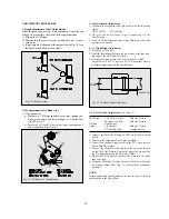
9. Transitional Operation Confirmation (Review to Play)
(Fig. 18)
Test Points:
CTL Pulse Test Pin
Path Adj. Fixture
Envelope Test Pin
Path Adj. Fixture
Observe:
Oscilloscope
Adjust:
VR Control
Path Adj. Fixture
S/T Guide Rollers
Transport Mech.
1).Connect the Path Adj. Fixture to PT01 on the Main circuit
board.
2).Play back the Alignment Tape (color bar alignment).
3).Connect the channel-1 scope probe to the CTL pulse test pin
on the Path Adj. Fixture.
4).Connect the channel-2 scope probe to the envelope test pin on
the Path Adj. Fixture. Externally trigger the scope using the
SW pulse test pin on the Path. Adj. Fixture.
5).Adjust the VR Control on the Path Adj. Fixture so that the
envelope signal of the test tape is maximum.
6).Operate VCR in the Review mode for approximately 15 sec-
onds and then change the mode to the Play mode.
7).Confirm that Within three (3) seconds the envelope waveform
is recovered when the mode changes from Review to Play
mode.
8).If the waveform is not recovered within the three (3) seconds
when the mode changes from Review to Play mode, make
sure that the tape runs smoothly at the lower Flange of T
Guide Post. And slightly adjust the S/T Guide Rollers to
amend the problem.
Fig. 16 Fine Adjustments of Drum Entrance/Exit
Envelopes
Fig. 17 Fine Adjustment of Envelopes at Drum
Entrance/Exit Parts
Fig. 18 Transitional Operation confirmation
(Review to Play)
Summary of Contents for DV- K504N-SJ
Page 35: ...34 AC001 K584NZ SJ M K584NZ SG M only...
Page 36: ...35...
Page 37: ...36...
Page 38: ...37...
Page 39: ...38...
Page 60: ...59 ELECTRICAL ADJUSTMENTS Fig 1 Circuit Board Location...
Page 92: ...91 INTERCONNECT WIRING DIAGRAM K584N K484N K384N K284N...
Page 93: ...92 POWER SUPPLY SCHEMATIC DIAGRAM FREE VOLTAGE K584NY SJ M K584NZ SJ M K584NZ SG M...
Page 95: ...94 2HD HEAD AMP SCHEMATIC DIAGRAM K384N K284N K304N...
Page 96: ...95 4HD HEAD AMP SCHEMATIC DIAGRAM K584N K484N K504N...
Page 97: ...96 VIDEO AUDIO SCHEMATIC DIAGRAM K584N K484N K384N K284N K504N K304N...
Page 98: ...97 PIF INPUT SELECTOR SCHEMATIC DIAGRAM 9V USE K584NY SJ M K584NZ SJ M K584NZ SG M...
Page 100: ...99 TIMER SYSCON SCHEMATIC DIAGRAM K584N K484N K384N K284N K504N K304N...
Page 101: ...100 POWER SUPPLY BLOCK DIAGRAM FREE VOLTAGE K584NY SJ M K584NZ SJ M K584NZ SG M...
Page 103: ...102 2HD HEAD AMP BLOCK DIAGRAM K384N K284N K304N...
Page 104: ...103 4HD HEAD AMP BLOCK DIAGRAM K584N K484N K504N...
Page 105: ...104 VIDEO AUDIO BLOCK DIAGRAM K584N K484N K384N K284N K504N K304N...
Page 106: ...105 PIF INPUT SELECTOR BLOCK DIAGRAM K584N K484N K384N K284N K504N K304N...
Page 109: ...108 MAIN PCB 2HEAD 4HEAD...


