50
3. VIDEO & AUDIO CIRCUIT
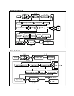
1) Video circuit
!
!
EEmode
1.0V Vp-p video signal out of jack or TMI (Tuner, modulator, If) is input to SW IC151.
One of them is selected and output to Pin 14 and them input to Pin 42 of IC301 (LA71004) for video signal process. This signal is
amplified 6dB through sync and peak AGC (Auto Gain Control) and 2Vp-p signal is output Pin 39 through QV/QH Insert circuit.
It is also output to Pin 5 of TMI and line jack.
@
@
REC mode
A. Luminance Signal Processing
The signal input by pin 42 of IC301 is input to AGC AMP and controls sync level. And then, it is input to first LPF (Fc=6MHz) with
limiting its band.
The signal out of the first LPF is separated into luminance and color signal by comb filter.
The separated luminance signal is passed through 3M LPF and pin 29 and buffer, and is input to pin 30.
The level is clamped in clamp circuit, which fixes sync to a specific level in order to prevent drift of FM frequency.
The edge of the clamped signal is emphasized by Detail Enhancer.
The emphasized signal is supplied to Non-Linear Emphasis circuit for improving S/N. Non-Linean Emphasis circuit adjusts amount of
emphasis, that is, makes it smaller in high frequency and vice versa in low frequency.
Main Emphasis emphasizes the high frequency of the adjusted signal again.
W/D clip is conducted in order to prevent undershoot and overshoot which are occurred during the above emphasizing process.
The luminance signal modulated by FM modulator is passed through REC-EQ and then output to pin 14 and then is input to pin 11 of ICA01.
ICA01 makes the luminance signal mixed with the down-converted 629KHz color signal input through pin 10, and also makes them
amplified. Then it supplies the signal through pin 17 in SP or pin 18 in SLP, into head.
Finally the signal comes to be recorded on a tape.
B. Color Signal Processing
The video signal input by pin 42 of IC301 passes through AGC AMP and 6MHz LPF.
Color signal and Y signal are separated by COMB FILTER and the color signal only passes through 3.58 BPF.
ACC AMP automatically controls burst level.
After Burst Emphasis boosts burst signal 6dB, 3.58MHz carrier is input to main conventer and is mixed with 4.21MHz carrier out of
subconverter.
The output is 4.21±3.58MHz.
The down converted 629KHz color signal, difference between the two frequencies, passes through 1.3MHz LPF, is output by pin 11 of
IC301, is input to pin 10 of ICA01, and is mixed with FM modulated luminance signal input by pin 11.
It is supplied to head and is recorded on a tape.
#
#
PB mode
A. Luminance Signal Processing
The recorded video signal picked up by head, is amplified 60dB by ICA01.
The amplified FM signal is output through pin 10 of ICA01 and input to pin 15 of IC301.
FM EQ and 629KHz trap of IC301 eliminates colors and passes only Y signal, which is output to pin 18 and 20, and is input to pin 22
after phase compensation.
After FM AGC automatically controls playback output tolerence of CH1 and CH2, it is sent to double limitter circuit which removes
AM noise and prevents overmodulation and lets the signal input to FM DEMOD which changes FM signal in record mode to the video
signal.
When it is recorded in main deemphasis through SUB LPF the boosted high frequency is deemphasized, passed through pin 29 and
buffer, and input to pin 30.
After 3MHz LPF's elminating demoduation noise during the above processes, it is input to YNR circuit.
The signal goes to CCD IC302 through pin 34, becomes 1H-delayed there, and then returns to YNR circuit through pin 32.
The 1H-delayed signal is mixed with signals inside of YNR, and as the result noise is eliminated.
Non-Linear Deemphasis plays a role quite opposed to Non-Linear Emphasis in record mode, that is, it deemphasized the high frequency
level emphasized by Non-Linear Emphasis.
Double Noise Canceller reduces minute noise of video signal. After passing through picture control block, it is mixed with color signal.
The mixed signal are output through pin 39, input to pin 18 of ICS01 output through pin 16, and finally supplied to both line jack and
pin 5 of TMI.
Summary of Contents for DV- K504N-SJ
Page 35: ...34 AC001 K584NZ SJ M K584NZ SG M only...
Page 36: ...35...
Page 37: ...36...
Page 38: ...37...
Page 39: ...38...
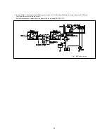
Page 60: ...59 ELECTRICAL ADJUSTMENTS Fig 1 Circuit Board Location...
Page 92: ...91 INTERCONNECT WIRING DIAGRAM K584N K484N K384N K284N...
Page 93: ...92 POWER SUPPLY SCHEMATIC DIAGRAM FREE VOLTAGE K584NY SJ M K584NZ SJ M K584NZ SG M...
Page 95: ...94 2HD HEAD AMP SCHEMATIC DIAGRAM K384N K284N K304N...
Page 96: ...95 4HD HEAD AMP SCHEMATIC DIAGRAM K584N K484N K504N...
Page 97: ...96 VIDEO AUDIO SCHEMATIC DIAGRAM K584N K484N K384N K284N K504N K304N...
Page 98: ...97 PIF INPUT SELECTOR SCHEMATIC DIAGRAM 9V USE K584NY SJ M K584NZ SJ M K584NZ SG M...
Page 100: ...99 TIMER SYSCON SCHEMATIC DIAGRAM K584N K484N K384N K284N K504N K304N...
Page 101: ...100 POWER SUPPLY BLOCK DIAGRAM FREE VOLTAGE K584NY SJ M K584NZ SJ M K584NZ SG M...
Page 103: ...102 2HD HEAD AMP BLOCK DIAGRAM K384N K284N K304N...
Page 104: ...103 4HD HEAD AMP BLOCK DIAGRAM K584N K484N K504N...
Page 105: ...104 VIDEO AUDIO BLOCK DIAGRAM K584N K484N K384N K284N K504N K304N...
Page 106: ...105 PIF INPUT SELECTOR BLOCK DIAGRAM K584N K484N K384N K284N K504N K304N...
Page 109: ...108 MAIN PCB 2HEAD 4HEAD...


