10
ELECTRICAL ADJUSTMENT
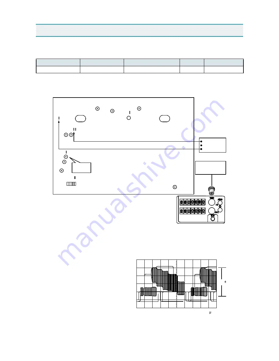
(4) FM DEVIATION
v
CONNECTION METHOD
v
ADJUSTMENT PROCEDURE
1) Supply the Color Bar Signal to the VIDEO IN JACK, and set the VCR to the REC mode.
2) Connect the oscilloscope to TJ396 and trigger scope with a composite sync signal at TJ302.
3) Record the Color Bar Signal for a few minute and
playback it. Then confirm that the playback video
output level (TJ396) is 2.0
±
0.2Vp-p.
4) Adjust as follows if the playback video output level
is not 2.0
±
0.2Vp-p.
4-1) Adjust R392 a little.
4-2) Record the Color Bar Signal for a few minute
and playback it.
4-3) Confirm the playback video output level.
4-4) Repeat the procedure of 4-1) to 4-3) until
the playback video output level becomes 2.0
( 0.2Vp-p between sync tip and 100% white
level.
Adjustment Parts
Check Point
Measuring Equipment
Test Tape
Input Signal
R392
TJ396
Signal Gen. Oscilloscope
Blank Tape
Color Bar
2.0V 0.2Vp-p
TJ396
Horizontal :10 s/div
Vertical :0.5V/div
FM DEV
TJ396
TJ302
CH-1
Oscilloscope
CH-2
SIGNAL
GENERATOR
R392
Summary of Contents for DV-K580NZ-T
Page 51: ...50 1 CONNECTION DIAGRAM CIRCUIT DIAGRAM...
Page 52: ...51 CIRCUIT DIAGRAM 2 POWER CIRCUIT DIAGRAM...
Page 53: ...52 CIRCUIT DIAGRAM 3 SYSCON CIRCUIT DIAGRAM...
Page 54: ...53 CIRCUIT DIAGRAM 4 VIDEO CIRCUIT DIAGRAM...
Page 55: ...54 CIRCUIT DIAGRAM 5 HEADAMP CIRCUIT DIAGRAM...
Page 56: ...55 CIRCUIT DIAGRAM 6 OSD CIRCUIT DIAGRAM...
Page 57: ...56 CIRCUIT DIAGRAM 7 Y C SEPARATION CIRCUIT DIAGRAM...
Page 58: ...57 CIRCUIT DIAGRAM 8 AUDIO CIRCUIT DIAGRAM...
Page 59: ...58 CIRCUIT DIAGRAM 9 LOGIC CIRCUIT DIAGRAM...
Page 60: ...59 CIRCUIT DIAGRAM 10 TERMINAL CIRCUIT DIAGRAM...
Page 61: ...60 COMPONENTS LOCATION GUIDE ON PCB BOTTOM VIEW 1 PCB MAIN...
Page 62: ...61 COMPONENTS LOCATION GUIDE ON PCB BOTTOM VIEW 2 PCB UNION...
Page 63: ...62 DISASSEMBLY 1 PANEL FRONT ASS Y...
Page 64: ...63 DISASSEMBLY 2 SET TOTAL ASS Y...
Page 65: ...64 DISASSEMBLY 3 PACKING ASS Y...


