25
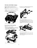
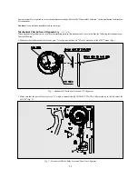
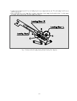
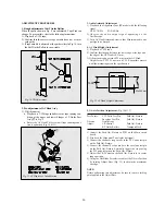
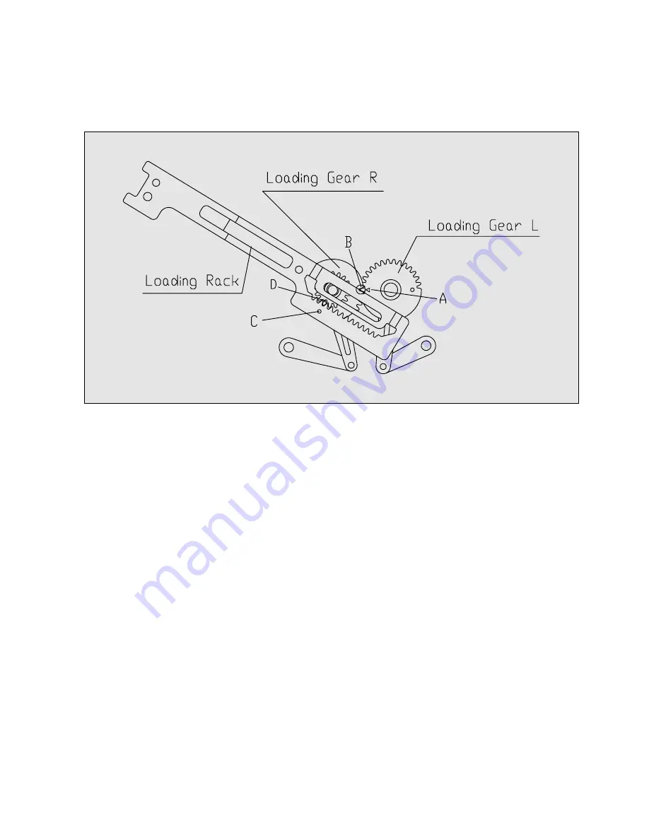
5. Confirm that the triangular mark "A" on the Loading Gear L Ass'y is aligned with the notch "B" in the Loading Gear R Ass'y in
EJECT mode (Fig. 5).
6. Make sure that the teeth of the Loading Rack are aligned with the those of the Loading Gear R so that the hole "C" of the Loading
Rack aligns with the circular mark "D" on the Loading Gear R (Fig. 5).
Fig. 5 - Mechanical Checks/Loading Loading Rack and Loading Gear Alignment
Summary of Contents for DV- K584N-SJ
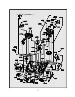
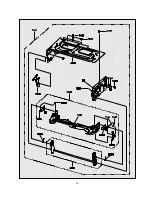
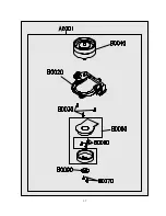
Page 35: ...34 AC001 K584NZ SJ M K584NZ SG M only...
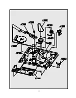
Page 36: ...35...
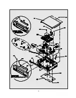
Page 37: ...36...
Page 38: ...37...
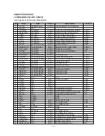
Page 39: ...38...
Page 60: ...59 ELECTRICAL ADJUSTMENTS Fig 1 Circuit Board Location...
Page 92: ...91 INTERCONNECT WIRING DIAGRAM K584N K484N K384N K284N...
Page 93: ...92 POWER SUPPLY SCHEMATIC DIAGRAM FREE VOLTAGE K584NY SJ M K584NZ SJ M K584NZ SG M...
Page 95: ...94 2HD HEAD AMP SCHEMATIC DIAGRAM K384N K284N K304N...
Page 96: ...95 4HD HEAD AMP SCHEMATIC DIAGRAM K584N K484N K504N...
Page 97: ...96 VIDEO AUDIO SCHEMATIC DIAGRAM K584N K484N K384N K284N K504N K304N...
Page 98: ...97 PIF INPUT SELECTOR SCHEMATIC DIAGRAM 9V USE K584NY SJ M K584NZ SJ M K584NZ SG M...
Page 100: ...99 TIMER SYSCON SCHEMATIC DIAGRAM K584N K484N K384N K284N K504N K304N...
Page 101: ...100 POWER SUPPLY BLOCK DIAGRAM FREE VOLTAGE K584NY SJ M K584NZ SJ M K584NZ SG M...
Page 103: ...102 2HD HEAD AMP BLOCK DIAGRAM K384N K284N K304N...
Page 104: ...103 4HD HEAD AMP BLOCK DIAGRAM K584N K484N K504N...
Page 105: ...104 VIDEO AUDIO BLOCK DIAGRAM K584N K484N K384N K284N K504N K304N...
Page 106: ...105 PIF INPUT SELECTOR BLOCK DIAGRAM K584N K484N K384N K284N K504N K304N...
Page 109: ...108 MAIN PCB 2HEAD 4HEAD...

