31
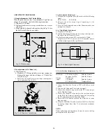
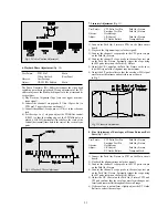
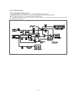
6. Playback Phase Adjustment (Fig. 14)
Test Points:
PT01 Pin3
Main
Video Out Jack
Rear Panel
Observe:
Oscilloscope
Adjust:
VR595 (PG Shifter)
Main
The Phase Generator (PG) Shifter determines the video head
switching point during playback. Wrong adjustment of the PG
shifter may cause the head switching noise in the picture and/or
vertical jitter.
1). Play Back the Alignment Tape (color bar signal or mono-
scope signal).
2). Connect the channel-1 scope probe (1V/div.: 50psec/div.) to
PT01 pin3. Trigger the scope on channel-1.
3). Connect the channel-2 scope prove (1V/div.) to the video out
jack.
4). Set the scope to (–) slope an adjust the PG Shifter control
(VR595) so that the trailing edge of the SW30Hz pulse is
placed 6.5H±0.5H(horizontal) lines before the start of the
vertical (horizontal) lines before the start of the vertical sync
pulse.
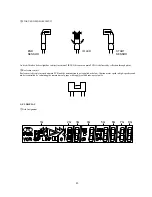
7. Linearity Adjustment (Fig. 15)
Test Points:
CTL Pulse Test Pin
Path Adj. Fixture
Envelope Test Pin
Path Adj. Fixture
Observe:
Oscilloscope
Adjust:
VR Control
Path Adj. Fixture
S/T Guide Rollers
Transport Mech.
1). Connect the Path Adj. Fixture to PT01 on the Main circuit
board.
2). Play back the Alignment tape (color bar signal).
3). Connect the channel-1 scope probe to the CTL pulse test pin
on the Path Adj. Fixture.
4). Connect the channel-2 scope probe to the envelope test pin
on the Path Adj. Fixture. Externally trigger the scope using
the SW pulse test pin on the Path Adj. Fixture.
5). Adjust the VR Control on the Path Adj. Fixture so the enve-
lope (FM) signal of the Aligment tape is maximum.
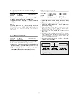
6). Adjust the S/T guide rollers so that the envelope (FM) signal
waveform at the entrance and exit sides are as shown
in Fig. 1
8. Fine Adjustment of Envelopes at Drum Entrance/Exit
Parts (Fig. 16 & 17)
Test Points:
CTL Pulse Test Pin
Path Adj. Fixture
Envelope Test Pin
Path Adj. Fixture
Observe:
Oscilloscope
Adjust:
VR Control
Path Adj. Fixture
S/T Guide Rollers
Transport Mech.
1).Connect the Path Adj. Fixture to PT01 on the Main circuit
board.
2). Play back the alignment tape (color bar signal).
3). Connect the channel-1 scope probe to the CTL pulse test pin
on the Path Adj. Fixture.
4). Connect the channel-2 scope probe to the envelope test pin
on the Path Adj. Fixture. Externally trigger the scope using
the SW pulse test pin on the Path Adj. Fixture.
5). Adjust the VR Control on the Path Adj. Fixture CCW and
CW and confirm that the envelope waveform changes uni-
formly and remains flat throughout the overall range.
6). If the envelope is not uniform, slightly adjust the S/T Guide
Rollers to correct the envelope.
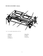
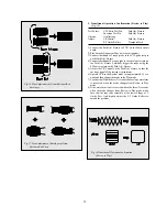
Fig. 13 X-Axis Position Adjustment
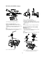
Fig. 14 Playback Phase Adjustment
Fig. 15 Linearity Adjustment
Summary of Contents for DV- K584N-SJ
Page 35: ...34 AC001 K584NZ SJ M K584NZ SG M only...
Page 36: ...35...
Page 37: ...36...
Page 38: ...37...
Page 39: ...38...
Page 60: ...59 ELECTRICAL ADJUSTMENTS Fig 1 Circuit Board Location...
Page 92: ...91 INTERCONNECT WIRING DIAGRAM K584N K484N K384N K284N...
Page 93: ...92 POWER SUPPLY SCHEMATIC DIAGRAM FREE VOLTAGE K584NY SJ M K584NZ SJ M K584NZ SG M...
Page 95: ...94 2HD HEAD AMP SCHEMATIC DIAGRAM K384N K284N K304N...
Page 96: ...95 4HD HEAD AMP SCHEMATIC DIAGRAM K584N K484N K504N...
Page 97: ...96 VIDEO AUDIO SCHEMATIC DIAGRAM K584N K484N K384N K284N K504N K304N...
Page 98: ...97 PIF INPUT SELECTOR SCHEMATIC DIAGRAM 9V USE K584NY SJ M K584NZ SJ M K584NZ SG M...
Page 100: ...99 TIMER SYSCON SCHEMATIC DIAGRAM K584N K484N K384N K284N K504N K304N...
Page 101: ...100 POWER SUPPLY BLOCK DIAGRAM FREE VOLTAGE K584NY SJ M K584NZ SJ M K584NZ SG M...
Page 103: ...102 2HD HEAD AMP BLOCK DIAGRAM K384N K284N K304N...
Page 104: ...103 4HD HEAD AMP BLOCK DIAGRAM K584N K484N K504N...
Page 105: ...104 VIDEO AUDIO BLOCK DIAGRAM K584N K484N K384N K284N K504N K304N...
Page 106: ...105 PIF INPUT SELECTOR BLOCK DIAGRAM K584N K484N K384N K284N K504N K304N...
Page 109: ...108 MAIN PCB 2HEAD 4HEAD...

