15
CIRCUIT
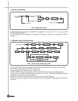
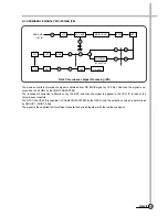
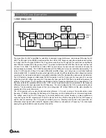
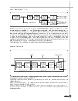
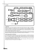
The circuitry of Normal AUDIO part is similar to that of the conventional Normal AUDIO part in case of EE and PB
mode, but in REC mode, due to the internal operation of self-alignment, it shows a lot of differences.
1. EE MODE
LA71511M has 3-input VIDEO/AUDIO switching circuitry internally, and its switching is controlled by the serial data
dispatched from MICOM.
But for the suitable operation to these models, only One input is used. The Normal AUDIO signal from Hi-Fi Audio
part is divided by the resistor, R202 and R203 and then supplied to the 73rd pin of LA71511M. Its level is
automatically controlled by ALC and then the amplified signal through LINE AMP is obtained at the 77th pin.
The signal from C208 is supplied to REC AMP after the divider circuit (R204, R205, R207) and also to the Hi-Fi IC
BH7804K.
The ALC point can be adjusted by R208 and R209, the adjustment of which is closely related to the REC level in
REC mode.
The ALC time can be adjusted by R201 and C201.
2. PB MODE
The PB signal picked up from AUDIO HEAD is firstly processed in the frequency characteristic compensator which is
composed of R220 and C214 (EP : C214+C215) and then supplied to the 7th pin.
The input signal passes through EQ AMP, and LINE AMP, so its output signal is finally obtained from the 77th pin.
The circuitry and its operation of EQ AMP is identical to the conventional EQ AMP.
3. REC MODE
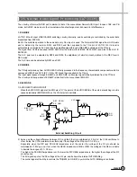
1) AUDIO SWITCHING CIRCUIT
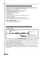
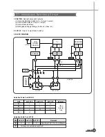
When the AUDIO S/W signal at the 80th pin is “H”, the point at the AUDIO HEAD of the external switching circuit is
opened electrically (EE/PB=GND), so the COIL starts to oscillate.
2) As long as the voltage difference between VCC and the 5th pin is maintained at 2.0~4.3V, the COIL oscillates. In
other words, the COIL maintains to oscillate only if the voltage at the 5th pin is 0.7~3.0V
p-p
.
Especially, when the R/P and FE HEAD impedance is at the center, the voltage at the 5th pin should be
maintained at 1.85V
p-p
, and, if not, when the HEAD impedance is MAX or MIN, the voltage at the 5th pin is liable
to deviate the ranges of 0.7~3.0V
p-p
.
The higher the FE HEAD impedance is or the lower the R/P HEAD impedance is, the higher the voltage at the 5th
pin increases.
The AC signal is put on the DC voltage at the 5th pin, and it shows the internal AUTO BIASing.
The control signal at the 6th pin controls the TR(Q205) to ON/OFF, by which the AUTO BIASing is controlled.
3-5. Normal Audio Signal Processing (LA71511M)
REC : OPEN
EE : GND
A-H
S/W
Q202
Q204
Q203
R/P
HEAD
R214
R216
R218
R217
VCC
R215
80
5
BIAS COIL
5th PIN
External Switching Circuit
Summary of Contents for DV-K88 series
Page 71: ...68 CIRCUIT DIAGRAMS 9 1 Connection Diagram SECTION 9 CIRCUIT DIAGRAM 68...
Page 72: ...69 CIRCUIT DIAGRAMS R819 5 1 9 2 Power Circuit Diagram...
Page 73: ...70 CIRCUIT DIAGRAMS 9 3 Syscon and Logic Circuit Diagram...
Page 74: ...71 CIRCUIT DIAGRAMS 9 4 AV SW Circuit Diagram...
Page 75: ...72 CIRCUIT DIAGRAMS 9 5 IF PDC Circuit Diagram TM...
Page 76: ...73 CIRCUIT DIAGRAMS 9 6 If Module Circuit Diagram A2...
Page 77: ...74 CIRCUIT DIAGRAMS 9 7 If Module Circuit Diagram Nicam...
Page 78: ...75 CIRCUIT DIAGRAMS 9 8 Hi Fi Pre Amp Circuit Diagram...
Page 79: ...76 CIRCUIT DIAGRAMS 9 9 Video Audio Circuit Diagram...
Page 80: ...77 CIRCUIT DIAGRAMS 9 10 Remocon Circuit Diagram...
Page 81: ...SECTION 10 COMPONENTS LOCATION GUIDE ON PCB BOTTOM VIEW 78 P C B LOCATION 10 1 PCB Main...
Page 82: ...80 P C B LOCATION 10 3 PCB Logic DV K8K S S Series DV K86 S S Series DV K82 S S Series...
Page 83: ...81 P C B LOCATION DV K88 S S Series...
Page 84: ...SECTION 11 DISASSEMBLY 83 DISASSEMBLY 11 1 Packing Ass y...
Page 85: ...84 DIAGRAMS DV K88 Series DV K82 Series DV K8K Series DV K86 Series 11 2 Front Panel Assembly...


