background image

Data sheet status 

Product specification 

The data sheet contains final product specifications. 

Limiting values 

Limiting values given are in accordance with the Absolute Maximum Rating System (IEC 134). 
Stress above one or more of the limiting values may cause permanent damage to the device. These 
are stress ratings only and operation of the device at these or any other conditions above those 
given in the Characteristics sections of the specification is not implied. Exposure to limiting values 
for extended periods may affect device reliability. 

Application information 

Where application information is given, it is advisory and dose not form part of the specification. 

Product Environmental certification 

ROHS 

REMARK 

All The specifications listed in this document are guaranteed for module only. Post-assembled 
operation or component(s) may impact module performance or cause unexpected effect or damage 
and therefore listed specifications is not warranted after any Post-assembled operation. 

GDEH075Z90

12

38

7.5 inch Series

www.good-display.com

GOOD DISPLAY

Summary of Contents for E-paper Series

Page 1: ...7 5 inch E paper Display Series GDEH075Z90 Dalian Good Display Co Ltd G O O D D I S P L A Y...

Page 2: ...05 25 Revision 1 2 Design Engineering Approval Check Design Zhongnan Building No 18 Zhonghua West ST Ganjingzi DST Dalian CHINA Tel 86 411 84619565 Fax 86 411 84619585 810 Email info good display com...

Page 3: ...ximum rating 3 2 DC Characteristics 3 3 Serial Peripheral Interface Timing 3 4 Power Consumption 4 Typical Operating Sequence 4 1 Normal Operation Flow 5 Command Table 6 Optical characteristics 6 1 Sp...

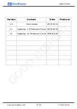
Page 4: ...ent Date Producer 1 0 New release 2019 10 14 GDEH075Z90 4 38 7 5 inch Series 1 1 Updating 1 6 Reference Circuit 2020 03 30 www good display com 1 2 Updating 1 6 Reference Circuit 2020 05 25 G O O D D...

Page 5: ...Ultra Low current deep sleep mode On chip display RAM Low voltage detect for supply voltage High voltage ready detect for driving voltage Internal temperature sensor 10 byte OTP space for module ident...

Page 6: ...677 3 RESOLUTION 528gate X 880source 4 pixel size O 1855mm X 0 1855mm 5 Unspecified Tolerance 0 20 6 Material conform to the ROHS standard 7 as the focus control si FPC PI Stiffener Total ThicknessO 3...

Page 7: ...BUSY Busy state output pin Note 1 5 4 10 RES Reset Note 1 5 3 11 D C Data Command control pin Note 1 5 2 12 CS Chip Select input pin Note 1 5 1 13 SCL serial clock pin SPI 14 SDA serial data pin SPI...

Page 8: ...al input The Reset is active low Note 1 5 4 This pin BUSY is Busy state output pin When Busy is High the operation of chip should not be interrupted and any commands should not be issued to the module...

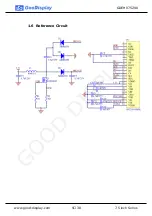
Page 9: ...1 6 Reference Circuit GDEH075Z90 9 38 7 5 inch Series www good display com G O O D D I S P L A Y...

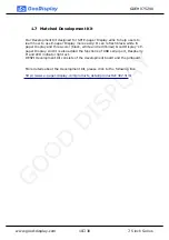
Page 10: ...red Yellow Good Display s E paper Display And it is also added the functions of USB serial port Raspberry Pi and LED indicator light ect DESPI Development Kit consists of the development board and the...

Page 11: ...is not applied to the module 2 It s recommended that you attach a transparent protective plate to the surface in order to protect the EPD Transparent protective plate should have sufficient strength i...

Page 12: ...the specification is not implied Exposure to limiting values for extended periods may affect device reliability Application information Where application information is given it is advisory and dose n...

Page 13: ...068 2 14NB 8 Package Vibration 1 04G Frequency 10 500Hz Direction X Y Z Duration 1hours in each direction Full packed for shipment 9 Package Drop Impact Drop from height of 100 cm on Concrete surface...

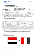
Page 14: ...ly for VSS 0V VCI 3 3V TOPR 25 Table 3 2 1 DC Characteristics Symbol Parameter Test Condition Applicable pin Min Typ Max Unit VCI VCI operation voltage VCI 2 2 3 3 7 V VIH High level input voltage SDA...

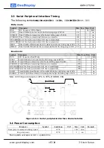
Page 15: ...Time CSB has to be low before the first rising edge of SCLK 100 ns tCSHLD Time CSB has to remain low after the last falling edge of SCLK 50 ns tCSHIGH Time CSB has to remain high between two transfer...

Page 16: ...interface SPI L Required Required Required SCL SDI SDO 3 wire serial peripheral interface SPI 9 bits SPI H Required Required L SCL SDI SDO 3 5 2 MCU Serial Peripheral Interface 4 wire SPI The 4 wire...

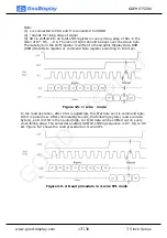
Page 17: ...Byte register according to D C pin Figure 3 5 1 wire mode In the read operation after CS is pulled low the first byte sent is command byte D C is pulled low After command byte sent the following byte...

Page 18: ...D7 bit D6 bit to D0 bit The first bit is D C bit which determines the following byte is command or data When D C bit is 0 the following byte is command When D C bit is 1 the following byte is data Tab...

Page 19: ...e send the following byte s are data byte s with D C bit is 1 After D C bit sending from MCU an 8 bit data will be shifted out on every clock falling edge The serial data output SDO bit shifting seque...

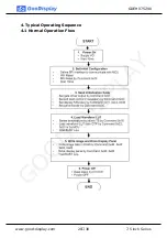
Page 20: ...4 Typical Operating Sequence 4 1 Normal Operation Flow GDEH075Z90 20 38 7 5 inch Series www good display com G O O D D I S P L A Y...

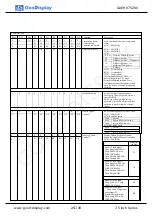
Page 21: ...G3 G2 B 1 SM Change scanning order of gate driver SM 0 POR G0 G1 G2 G3 679 left and right gate interlaced SM 1 G0 G2 G4 G678 G1 G3 G679 B 0 TB TB 0 POR scan from G0 to G679 TB 1 scan from G679 to G0 0...

Page 22: ...4h 4 6 C5h 7 9 A5h 4 7 C6h 8 A6h 4 8 C7h 8 1 A7h 4 9 C8h 8 2 A8h 5 C9h 8 3 A9h 5 1 CAh 8 4 AAh 5 2 CBh 8 5 ABh 5 3 CCh 8 6 ACh 5 4 CDh 8 7 ADh 5 5 CEh 8 8 AEh 5 6 Other NA 0 0 0F 0 0 0 0 1 1 1 1 Gate...

Page 23: ...per and lower bit of the address 00 Y decrement X decrement 01 Y decrement X increment 10 Y increment X decrement 11 Y increment X increment POR A 2 AM Set the direction in which the address counter i...

Page 24: ...arts BUSY pad will output high during detection The detection result can be read from the Status Bit Read Command 0x2F 0 1 0 0 0 0 0 A2 A1 A0 0 0 18 0 0 0 1 1 0 0 0 Temperature Sensor Control Temperat...

Page 25: ...lay Update A 7 0 00h POR A 7 4 Red RAM option 0000 Normal 0100 Bypass RAM content as 0 1000 Inverse RAM content A 3 0 BW RAM option 0000 Normal 0100 Bypass RAM content as 0 1000 Inverse RAM content 0...

Page 26: ...re value from I2C Single Master Interface B9 Then Load LUT with DISPLAY Mode 2 To Disable Clock Signal Enable ANALOG Then DISPLAY with DISPLAY Mode 1 47 Then Disable ANALOG Then Disable OSC Enable ANA...

Page 27: ...ister 41h to select reading RAM BW RAM RED until another command is written Address pointers will advance accordingly The 1st byte of data read is dummy data 0 0 28 0 0 1 0 1 0 0 0 VCOM Sense Enter VC...

Page 28: ...1 3 84 3 3 38h 1 4 88 3 4 3Ch 1 5 8C 3 5 40h 1 6 90 3 6 44h 1 7 94 3 7 48h 1 8 98 3 8 4Ch 1 9 9C 3 9 50h 2 A0 4 54h 2 1 0 0 2D 0 0 1 0 1 1 0 1 OTP Register Read for Display Option Read Register for Di...

Page 29: ...0 Display Mode for WS 35 32 0 Display Mode 1 1 DisplayMode2 F 6 PingPong for Display Mode 2 F 7 PingPong for Display Mode 1 1 Ping Pong 0 Default G 7 0 J 7 0 module ID waveform version Remarks A 7 0 J...

Page 30: ...0 1 Read RAM Option Read RAM Option A 0 0 POR 0 Read RAM corresponding to 24h 1 Read RAM corresponding to 26h 0 1 0 0 0 0 0 0 0 A0 0 0 44 0 1 0 0 0 1 0 0 Set RAM X address Start End position Specify...

Page 31: ...X direction according to Source BUSY pad will output highduring operation 0 1 A7 A6 A5 A4 0 A2 A1 A0 0 0 47 0 1 0 0 0 1 1 1 Auto Write B W RAM for Regular Pattern Auto Write B W RAM for Regular Patte...

Page 32: ...A9 A8 0 0 4F 0 1 0 0 1 1 1 1 Set RAM Y address counter Make initial settings for the RAM Y address in the address counter AC A 9 0 000h POR 0 1 A7 A6 A5 A4 A3 A2 A1 A0 0 1 0 0 0 0 0 0 A9 A8 0 0 7F 0 1...

Page 33: ...5 Note 6 1 1 WS White State L value 63 65 Note 6 1 1 RS Red State L value Red 25 28 Note 6 1 1 Red State a value Red 36 40 Note 6 1 1 Panel s life 0 40 5years Note 6 1 2 Panel Image Update Storage and...

Page 34: ...ction Ratio The reflection ratio is expressed as R Reflectance Factor white board x L center L white board L center is the luminance measured at center in a white area R G B 1 L white board is the lum...

Page 35: ...w Not Allow Ignore Display error Electric Display Not Allow Not Allow Ignore Scratch or line defect include dirt Visual Film card L 2 W 0 1 Ignore Ignore 1 0mm L 9 0mm 0 1 W 0 2mm N 2 Ignore L 9 0 W 0...

Page 36: ...L long W wide D point size GDEH075Z90 36 38 7 5 inch Series www good display com G O O D D I S P L A Y...

Page 37: ...8 Packing GDEH075Z90 37 38 7 5 inch Series www good display com G O O D D I S P L A Y...

Page 38: ...wn as Ghosting or Image Sticking may occur It is recommended to refreshed the ESL EPD Tag every 24 hours in use case It is recommended that customer ships or stores the ESL EPD Tag with a completely w...

Reviews: