PCIe-FRM24 Users Manual (Rev 1.3)
-
15-
http://www.daqsystem.com
CCx+
CCx-
Camera Control
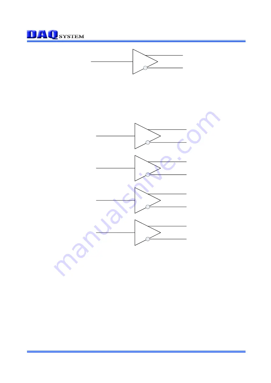
Above picture is a Camera Control output circuit from PCIe-FRM24 board to Camera for the
specific control of the Camera-link Cable.
The PCIe-FRM24 board has four differential digital outputs. Each output is mapped by Digital
output. Below picture display that each bit position set.
CC1+
CC1-
CC_D0
CC2+
CC2-
CC_D1
CC3+
CC3-
CC_D2
CC4+
CC4-
CC_D3
[Figure 3-5. Camera Control LVDS Digital Output Circuit]
3.3.3 J1 Connector (2Pin Header, 2.54mm)
3.3V external DC power connector. It is a power source for FPGA installation and is not
normally used.
3.3.4 J5 Connector
J5 is a Joint Test Action Group (JTAG) connector used to update the FPGA program on the
board. It does not use when operating the board normally.


