background image


PCI-EK01 Users Manual (Rev 1.0) 


                                                                  -

27-                                                     

http://www.daqsystem.com


Windows XP Professional or Windows 2000 

6. Refer to AN203(PCI-EK01-Register Level Application Guide) 


4.1 Analog Output 

(1) 

DAC FIFO Write Points 

input 

“1000” and press

 DAC test(DAC FIFO Write) 

button. It will record a 

  sine wave data of 1000 points for making waveform at DAC FIFO. 

The 1000 points is a data from DAC channel 0 ~ 3. 

(2) After 

I/O address offset

 input 

“94 and 

Data 

input 

“1”, press 

I/O Write

 button. 

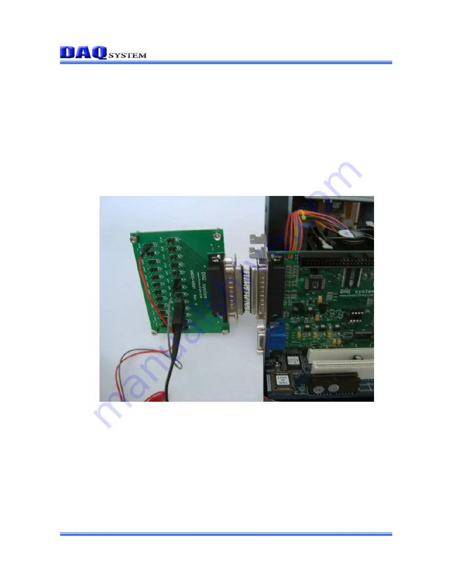
(3) User confirm whether or not sine  wave  is  displayed on  P1(D-sub  25pin plug)  connector as  it use 

Oscilloscope like Figure 4-2. 


[Figure 4-2. Connection for Test] 

Summary of Contents for PCI-EK01

Page 1: ...ystem is believed to be accurate and reliable However no responsibility is assumed by DAQ system for its use nor for any infringements of patents or other rights of third parties which may result from...

Page 2: ...tware installation 3 PCI EK01 Board Explanation 3 1 PCI EK01 Function 3 2 Address Map 3 3 Jumper Option and Connector Pin out 3 4 CDROM Folder 4 Sample Program Test 4 1 Analog Output 4 2 Analog Input...

Page 3: ...Analog Converter high current driver and high speed analog data logger Figure 1 1 PCI EK01 Functional Blocks PRODUCT INFORMATION Application PCI development and evaluation Data acquisition Laboratory...

Page 4: ...n 4 channel output 0 to 3 3V output range MAX 1M 1uSEC update rate Can change update interval in waveform generation mode by 1uSEC increment Simultaneous update of outputs 16 LSB INL 1 LSB DNL 3 LSB O...

Page 5: ...1 PCI EK01 Board 2 Windows2000 XP Driver CDROM 3 Application Sample Source CDROM 4 Schematic Part List etc CDROM 2 2 Hardware Installation For PCI EK01 board installation to PC is as follows There isn...

Page 6: ...he switch after assembly Figure 2 2 PCI EK01 connect to PC Above picture shows no PC case for user understanding Generally it use in case of PC mother board 5 When the power on two LED is lighting on...

Page 7: ...e isn t special explanation 1 After finished booting that you can show the picture of Found New Hardware Wizard window Select the item Install from a list or specific location Advanced and click Next...

Page 8: ...Rev 1 0 8 http www daqsystem com Figure 2 4 PCI EK01 Device Driver Search Window A warning message appears during installation here press Continue Anyway button You can show below message window Proce...

Page 9: ...ting Device Driver Window 4 If the installation is completely finished you can use the USB DIO6400 board But it confirm a driver normally installation in the following ways Do the following steps to s...

Page 10: ...m com Figure 2 7 Device Manager window If you can see the PCI EK01 at Multifunction Adaptors the driver installation is to have been over Check the red circle Important Notice After installation you s...

Page 11: ...hat the PCI EK01 has a lot of functions for various test Each configuration function is as follows 1 Core Control The PCI EK01 composes a PCI Target external ADC DAC interface and FIFO TIMER Counter w...

Page 12: ...8bits of these 24bits can drive 500mA 6 SRAM It is used to high speed data transfer Max 33Mhz and ADC s data buffer as it equip maximum 8Mbit 1M Byte high speed RAM 7 T Rx It is a RS232C Transceiver I...

Page 13: ...urce and device state control register etc Memory Area I O Area Configuration Area 4G 64K 64DWORD Figure 3 2 Address Map of IBM PC Series The PCI EK01 use a memory and I O that have been assigned to s...

Page 14: ...Manual Rev 1 0 14 http www daqsystem com Figure 4 3 PCI EK01 Address map Notice 1 Currently it is not used a UART function it will be upgrade later 2 Currently it is not used a VGA function it will be...

Page 15: ...nnection for special test Yhis chapter will be explained this situation JP4 JP5 JP2 JP12 JP11 JH1 JP1 P1 P2 JP3 LED4 JP6 JP8 JP9 JP7 JP13 JP10 SW1 SW2 SW3 SW4 SW5 COM1 LED1 LED2 LED3 LED5 LED6 LED7 Y1...

Page 16: ...used 15 JP12 PCI I O Power Not used 16 JP13 User defined Jumper Connection Tact Switch 17 LED1 3 LED5 For PCI Transition Monitor 18 LED4 FPGA configuration Indicator 19 LED6 Clock Indicator 20 LED7 P...

Page 17: ...og Ground in case of external interface of an analog signal 3 10 9 8 7 6 1 2 5 4 19 18 17 16 15 14 13 12 11 25 24 23 22 21 20 Analog Power 3 3V Analog Input 1 Analog Input 7 Analog Input 5 Analog Inpu...

Page 18: ...8 http www daqsystem com P2 Description It is not used currently a VGA Video signal it will be upgrade 3 10 9 8 7 6 1 2 5 4 15 14 13 12 11 BLUE GREEN RED VSYNC HSYNC VGND VGND VGND VGND VGND Figure 3...

Page 19: ...56 53 54 63 64 61 DATA 0 DATA 1 DATA 2 DATA 3 DATA 4 DATA 5 DATA 6 DATA 7 DATA 8 DATA 9 DATA 10 DATA 11 DATA 12 DATA 13 DATA 14 DATA 15 BYTE EN1 LOW BYTE EN1 HIGH OE ADDRESS 00 ADDRESS 01 ADDRESS 02 A...

Page 20: ...8 7 6 1 2 5 4 19 18 17 16 15 14 13 12 11 24 23 22 21 20 PVCC 3 3V 5V PVCC 3 3V 5V 33 32 31 30 29 28 27 26 25 38 37 36 35 34 40 39 PORTB 0 PORTB 1 PORTB 2 PORTB 3 PORTB 4 PORTB 5 PORTB 6 PORTB 7 Digita...

Page 21: ...1 0 Master Parallel 0 1 1 Slave Parallel 1 0 1 JTAG 1 When connect jumper it is 0 2 A signal HSWAP_EN has an internal pull up resistor When connect jumper it is 0 If it is 0 an I O pin is pull up duri...

Page 22: ...ion 2 3 A JP4 can select DVCC or AVCC to the power of DAC chip The last jumper JP5 JP6 likes to use it with default setting as it refers to a schematic 3 1 2 3 1 2 3 1 2 JP4 JP5 JP3 3 1 2 JP9 RS232C I...

Page 23: ...source that user can install and test and program at PC First the drivers folder has Driver and Install File the manual folder has User Manual Schematic Application Note etc The Sample folder has som...

Page 24: ...The SAMPLE folder of CDROM includes a execution file and source file of PCITest exe The sample source files can use that a user modifies in order to implement a necessary function 1 2 3 4 5 6 7 8 9 1...

Page 25: ...record to a specific address of memory it is a value of offset 16bit Hexa Decimal 6 Memory Write Data The data that will be written to a specific address of memory When the data record to a specific...

Page 26: ...y It marks 4 channels at program 20 Time Knob It set up an axis of time if it marks ADC value to a screen Not apply Currently 21 Voltage Knob It set up an axis of voltage if it marks ADC value to a sc...

Page 27: ...1000 and press DAC test DAC FIFO Write button It will record a sine wave data of 1000 points for making waveform at DAC FIFO The 1000 points is a data from DAC channel 0 3 2 After I O address offset i...

Page 28: ...system com Figure 4 3 Confirm an Analog Output 4 The output is displayed all 4 Analog out It confirms all 4 channels as it use Oscilloscope 5 You can use Wave form generator like Figure 4 4 for Wave f...

Page 29: ...ms that 0 to 0 address 3FFFF to a FFFFCh address whether or not a record is made to double word 4 I O address offset input 84 and Data input 44 after that press I O Write button Figure 4 5 DaqScope Pr...

Page 30: ...that current count make 1 4 It apply count pulse two times more It confirm count over occurrence as reading a STATUS register counter 0 and current counter value is 3 5 There is 3 Counter at PCI EK01...

Page 31: ...through 64pin header connector 3 3V operation user selectable oscillator Video interface type B only UART interface type B only 5 2 Hardware Analog input 12bit resolution 8 Single ended or 4 differen...

Page 32: ...ng or logic low Timer Counter Three 32 bit Timer Three 32 bit Counter Input frequency max 60Mhz 25n timer resolution One shot or alternate timer output mode 3 3V CMOS logic level I O interface Externa...

Page 33: ...em com 5 4 Physical Environment Dimensions Standard Universal 5V 3 3V PCI 32bit form factor 175mm x 95mm P1 P2 175 95 Temperature 0 to 70 operating 20 to 80 storage Relative Humidity 20 to 80 percent...

Page 34: ...1 PCI System Architecture MindShare Inc 2 PCI Local Bus Specification PCI SIG 3 PCI EK01 Register Level Application Guide DAQ system 4 PCI EK01 Driver Level Programming Guide DAQ system 5 General info...

Reviews: