D i d o H a r d w a r e M a n u a l
v . 1 . 0 . 5
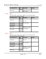
7.8.3
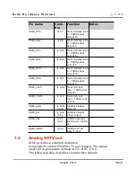
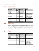
MMC/SD/SDIO2
The following table describes the interface signals:
Pin name
Conn.
Pin
Function
Notes
SD2_SCLK
J1.128 Clock output
SD2_CMD
J2.55
Command output
SD2_DAT[0]
J2.25
Data bit 0
Functions as single
data bit for 1-bit SD
mode.
SD2_DAT[1]
J2.24
Data bit 1
Functions as an IRQ
input for 1-bit SD
mode.
SD2_DAT[2]
J2.23
Data bit 2
Functions as a Read
Wait input for 1-bit
SD mode.
SD2_DAT[3]
J2.22
Data bit 3
7.9
USB ports
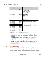
DIDO provides three USB 2.0 ports with integrated PHY. USB0
is a OTG 2.0 port, USB1 is a Host/OTG 2.0 port and USB2 is a
2.0 Host port. USB1 can be configured through dedicated
mount options. USB1 and USB2 are the downstreams of a USB
hub connected to the second USB controller provided by the
processor.
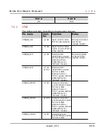
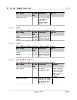
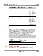
7.9.1
USB0
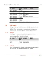
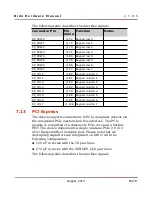
The following table describes the interface signals:
Pin name
Conn.
Pin
Function
Notes
USB0_DP
J1.6
Bidirectional data
differential signal
pair (plus/minus)
USB0_DM
J1.5
USB0_ID
J1.17
OTG identification
input.
USB0_VBUSIN
J1.16
5-V VBUS
comparator input.
Senses the level of
the USB VBUS.
Should connect
directly to the USB
VBUS voltage.
August, 2014
63/78


