background image

D i d o   H a r d w a r e   M a n u a l

v . 1 . 0 . 5

Connector Pin

Pin 
name

Function

Notes

J2.119

7.15

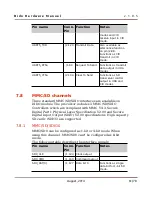
I2C buses

Two I2C channels are available on DIDO to provide an interface
to other devices compliant with Philips Semiconductors Inter-IC
bus (I2C-bus™) specification version 2.1. External components 
attached to this 2-wire serial bus can transmit/receive 8-bit 
data to/from the device through the I2C module. The I2C ports 
support standard and fast modes from 10 - 400 Kbps (no 
fail-safe I/O buffers).
A third I2C channel (I2C0) is used for the internal connection 
between CPU and PMIC (please refer to Section 5.2).

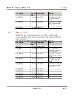
7.15.1 I2C2

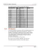
The following table describes the interface signals:

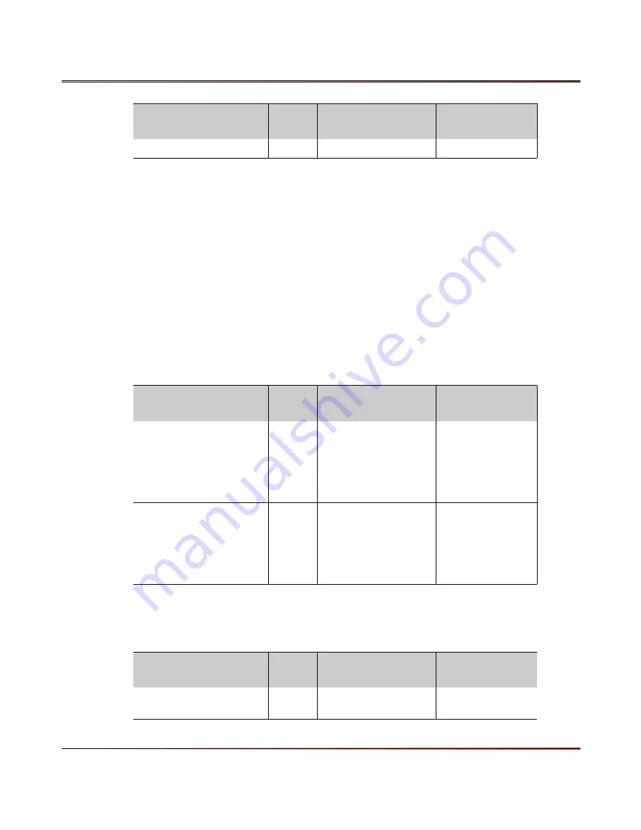
Connector Pin

Pin 
name

Function

Notes

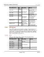
I2C[2]_SCL

J1.23

J2.122
J2.128

I2C2 Clock

For proper device
operation in I2C 
mode, this pin 
must be pulled 
up via
external resistor.

I2C[2]_SDA

J2.39
J2.66

J2.120
J2.121

I2C2 Data I/O

For proper device
operation in I2C 
mode, this pin 
must be pulled 
up via
external resistor.

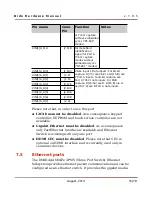
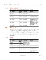
7.15.2 I2C3

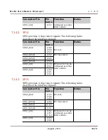
The following table describes the interface signals:

Connector Pin

Pin 
name

Function

Notes

I2C[3]_SCL

J2.106

J1.27

I2C3 Clock

J2.106 line is 
internally 

August, 2014

69/78

Summary of Contents for diDo

Page 1: ...HARDWARE MANUAL ARM Cortex A8 CPU Module Family DAVE Embedded Systems www dave eu info dave eu ULTRA Line...

Page 2: ...D i d o H a r d w a r e M a n u a l v 1 0 5 Page intentionally left blank August 2014 2 78...

Page 3: ...M387x CPU 16 3 2 DDR3 memory bank 18 3 3 NOR flash bank 18 3 4 NAND flash bank 18 3 5 Memory Map 19 3 6 Power supply unit 19 3 7 CPU module connectors 19 4 Mechanical specifications 21 4 1 Board Layou...

Page 4: ...9 7 3 Analog SDTV out 50 7 4 Digital Video Input ports 51 7 4 1 VIN0 52 7 4 2 VIN1 54 7 5 Ethernet ports 55 7 5 1 EMAC_RMREFCLK 56 7 5 2 Ethernet 10 100 56 7 5 3 Gigabit EMAC 57 7 6 CAN ports 58 7 6 1...

Page 5: ...2 Abbreviations and acronyms used in this manual 9 Tab 3 CPU Memories Busses 14 Tab 4 Peripherals 15 Tab 5 Electrical Mechanical and Environmental Specifications 15 Tab 6 DM814x AM387x comparison 18...

Page 6: ...VE Embedded Systems Srl is certified to ISO 9001 standards 1 4 Disclaimers DAVE Embedded Systems does not assume any responsibility about availability supplying and support regarding all the products...

Page 7: ...Embedded Systems that are caused by a faulty DIDO module 1 6 Technical Support We are committed to making our product easy to use and will help customers use our CPU modules in their systems Technica...

Page 8: ...h p DM814x_Overview Integration guide on DAVE Embedded Systems Developers Wiki http wiki dave eu index php Integrati on_guide_ 28Dido 29 Tab 1 Related documents 1 8 Conventions Abbreviations Acronyms...

Page 9: ...u a l v 1 0 5 Abbreviation Definition RTC Real time clock SOM System on module VIP Video Input Port PMIC Power Management Integrated Circuit ZFF Z Form Factor Tab 2 Abbreviations and acronyms used in...

Page 10: ...LK 4 0 0 Minor fixes 1 0 1 May 2013 Added information on EMAC_RMREFCLK signal Minor fixes 1 0 2 December 2013 Fixed JTAG_TDO and JTAG_TCK pinout table entries 1 0 3 January 2014 Updated pin J2 97 info...

Page 11: ...o surveillance cameras medical video analysis smart home controllers security systems automation and point of service DIDO is the first product of DAVE Embedded Systems ULTRA Line CPU modules class wh...

Page 12: ...abilities High Definition Video Image Coprocessing HDVICP v2 engine Multiple video input and output channels C674x DSP engine available on DM8148 NEON Multimedia co processor and PowerVR SGX 530 Vecto...

Page 13: ...D i d o H a r d w a r e M a n u a l v 1 0 5 2 2 Block DiagramBlock Diagram August 2014 13 78...

Page 14: ...ons Options Graphics Controller HD Video Processing Subsystem HDVPSS 1x up to 24 bit HD Video Output port 1x up to 18 bit HD Video Output port 1x HDMI 1 3 channel DDC Analog TV output TFT RGB support...

Page 15: ...o 1x McASP channel Timers Up to 6 programmable general purpose timers PWM function available RTC On board provided by TPS659113 PMIC external battery powered Debug JTAG EMU port Tab 4 Peripherals Feat...

Page 16: ...Instruments DaVinci digital media processor solutions are tailored for digital audio video imaging and vision applications Sitara ARM microprocessors MPUs are designed to optimize performance and per...

Page 17: ...performance floating point DSP generation in the TMS320C6000 DSP platform and is code compatible with previous generation C64x Fixed Point and C67x Floating Point DSP generation The C674x Floating Po...

Page 18: ...s CPU connection SDRAM bus Size min 128 MB Size max 2 GB Width 32 bit Speed 533 MHz Tab 7 DDR2 specifications 3 3 NOR flash bank NOR flash is a Serial Peripheral Interface SPI device By default this d...

Page 19: ...Wiki http wiki dave eu index php Memory_organization_ 28Dido 29 3 6 Power supply unit DIDO as the other Performance Line CPU modules embeds all the elements required for powering the unit therefore p...

Page 20: ...y on one module are replaced with different interfaces on the other modules As an example the following table reports the three configuration of pin J2 33 Module LIZARD NAON DIDO Pin J2 33 J2 33 J2 33...

Page 21: ...ristics of the DIDO module Mechanical drawings are available in DXF format from the DIDO page on DAVE Embedded Systems website http www dave eu dave cpu module am387x dm814x d ido html 4 1 Board Layou...

Page 22: ...v 1 0 5 Board height 59 7 mm Board width 68 6 mm Maximum components height is 3 1 mm PCB thickness is 1 8 mm The following figure highlights the maximum components heights on DIDO module August 2014...

Page 23: ...number Hirose FX8C 140S SV Height 5 6 mm Length 48 6 mm Depth 3 95 mm Mating connectors Hirose FX8C 140P SV 5 mm board to board height Hirose FX8C 140P SV1 6 mm board to board height Hirose FX8C 140P...

Page 24: ...n DIDO is powered this signal is low this means that carrier board 3 3V powered devices have to be powered off During power up sequence this signal shall be raised by DIDO circuitry indicating carrier...

Page 25: ...put signal acts as External Warm Reset It is connected to processor s RESETn pad Internal pullup is 2 2kOhm 5 3 5 JTAG_TRSTn J2 100 This input signal acts as Emulation Warm Reset It is connected to pr...

Page 26: ...MODE 10 0 XIP on GPMC Boot Options NO BTMODE 9 8 01 Ethernet PHY Mode Selection NO BTMODE 7 5 000 Reserved NO BTMODE 4 0 10111 Boot Mode Order YES Bootstrap pins BTMODE 4 0 are routed to main connecto...

Page 27: ...sequence customization The following reference schematic shows a simple resistor network that can be implemented on carrier board hosting DIDO module For each BTMODE 4 0 pin it is possible to populate...

Page 28: ...hen a simple procedure allow to load the 1st and 2nd stage bootloader from the serial line When the 2nd stage bootloader is running reprogramming the flash memory is straightforward The UART boot uses...

Page 29: ...guration is quite complex in DIDO but a tool from TI the Pin Mux Utility can help to perform this operation Software installation and generic usage documentation is available on this page of the TI Em...

Page 30: ...connected to the CAN transceiver PMIC x pin connected to the Power Manager IC LAN x pin connected to the LAN PHY USB x pin connected to the USB transceiver SV x pin connected to voltage supervisor MT...

Page 31: ...EMAC x Ethernet MAC x represents the port number 0 or 1 UART x UART port x represents the port number 0 to 5 GPx y General Purpose I O port x represents the port number 0 to 3 CAM Camera Interface SP...

Page 32: ...TSn UART4_TXD DCAN1_RX SPI 1 _SCS 2 n SD2_SDCD AF5 I O J1 21 UART0_CTSn DCAN1_TX CPU UART0_RTSn UART4_RXD DCAN1_TX SPI 1 _SCS 3 n SD0_SDCD AE6 I O J1 23 VIN0A_D16 CAM_D8 CPU VIN 0 A_D 16 CAM_D 8 I2C 2...

Page 33: ...0 _G_Y_YC 7 AD14 O RGB mode green YUV444 mode Y Y C mode Y J1 57 VOUT0_G_Y_YC5 CPU VOUT 0 _G_Y_YC 5 AB12 O RGB mode green YUV444 mode Y Y C mode Y J1 59 VOUT0_B_CB_C9 CPU VOUT 0 _B_CB_C 9 AG15 O RGB...

Page 34: ...EMAC_RMREFCLK TIM2_IO GP1 10 J27 I O Available on request module mount option Please refer to section 7 5 1 J1 93 USB0_DRVVBUS CPU USB0_DRVVBUS GP0 7 AF11 I O J1 95 USB1 VBUS CPU USB1_VBUSIN AG14 A I...

Page 35: ...D I O J1 8 UART0_TXD CPU UART0_TXD AG5 O 1 8V 3 3V J1 10 EEPROM_A0 EEPROM A1 A1 O J1 12 EEPROM_A1 EEPROM A2 A2 I O J1 14 MDIO_MDIO CPU MDIO GP1 12 P24 I O Module mount option UART4_TXD_GP3_2 CPU VOUT...

Page 36: ...0 VOUT0_R_CR4 CPU VOUT 0 _R_CR 4 AA9 O 1 8V 3 3V J1 52 DGND DGND G J1 54 VOUT0_G_Y_YC8 CPU VOUT 0 _G_Y_YC 8 AE14 O 1 8V 3 3V J1 56 VOUT0_G_Y_YC6 CPU VOUT 0 _G_Y_YC 6 AA8 O 1 8V 3 3V J1 58 VOUT0_G_Y_YC...

Page 37: ...EMAC 1 _ RMTXD 1 SPI 3 _D 1 GP0 16 AC21 I O J1 94 VIN0A_D23 CAM_D15 CPU VIN 0 A_D 23 CAM_D 15 EMAC 1 _ RMTXEN SPI 3 _D 0 GP0 17 AC16 I O J1 96 CAN_H CPU DCAN0_TX UART2_TXD I2C 3 _SDA GP1 0 AH6 I O J1...

Page 38: ...DGND G J1 128 SD2_SCLK CPU SD2_SCLK GP1 15 M23 I O 1 8V 3 3V J1 130 SD0_CMD CPU SD0_CMD SD1_CMD GP0 2 N1 I O 1 8V 3 3V J1 132 VIN1A_D0 GP3_0 CPU VOUT 1 _B_CB_C 3 EMAC 1 _MRCL K VIN 1 A_D 0 UART4_CTSN...

Page 39: ...DGND G 1 8V 3 3V J2 29 PCIE_TXP0 CPU PCIE_TXP0 AD2 O 1 8V J2 31 PCIE_TXN0 CPU PCIE_TXN0 AD1 O 1 8V J2 33 DGND DGND G 3 3V J2 35 3 3V 3V3 S J2 37 DGND DGND G J2 39 GPMC_A14 I2C2_SDA CPU VOUT 1 _R_CR 3...

Page 40: ...V J2 77 VIN0A_D8_BD0 GP2_13 CPU VIN 0 A_D 8 _BD 0 GP2 13 AB15 I O 1 8V 3 3V J2 79 VIN0A_D9_BD1 GP2_14 CPU VIN 0 A_D 9 _BD 1 GP2 14 AG9 I O 1 8V 3 3V J2 81 VIN0A_D10_BD2 GP2_15 CPU VIN 0 A_D 10 _BD 2 G...

Page 41: ...CS 1 n G P3 14 AG27 I O J2 113 SPI3_D1 UART3_RTSn GP2_ 29 CPU VOUT 1 _HSYNC EMAC 1 _MCOL VIN 1 A_VSYNC PATA_HDDIR SPI 3 _D 1 UART3_RTSn GP2 29 AC24 I O J2 115 EMAC0_PHY_LED_LINK ACT LAN LED1 3 J2 117...

Page 42: ...3 3V J2 20 DGND DGND G J2 22 GPMC_A1 SD2_DAT3 CPU SD2_DAT 3 GPMC_A 1 GP2 5 J28 I O 1 8V 3 3V J2 24 GPMC_A3 SD2_DAT1 CPU SD2_DAT 1 _SDIRQn GPMC_A 3 GP1 13 M24 I O 1 8V 3 3V J2 26 DGND DGND G J2 28 PCIE...

Page 43: ...VOUT0_R_CR3 GP2_27 CPU VOUT 0 _R_CR 3 GP2 27 AB9 I O 1 8V 3 3V Module mount option CORE_VDD MTR O J2 66 VOUT1_G_Y_YC3 GP3_7 GP3_23 CPU VOUT 1 _G_Y_YC 3 EMAC 1 _MR XD 6 VIN 1 A_D 8 GP3 7 Y23 EMAC 0 _MT...

Page 44: ...A 1 _AXR 7 T IM3_IO GP0 15 H2 I O 1 8V 3 3V J2 94 JTAG_RTCK CPU RTCK AD4 I 1 8V 3 3V J2 96 JTAG_TDO CPU TDO AC5 O 1 8V 3 3V J2 98 JTAG_TCK CPU TCK W7 I 1 8V 3 3V J2 100 JTAG_TRSTn CPU TRSTn AA4 I 1 8V...

Page 45: ...UART 1_TXD GP1 4 AG2 I O 1 8V 3 3V J2 132 VIN1A_D4 GP3_4 CPU VOUT 1 _B_CB_C 7 EMAC 1 _MR XD 3 VIN 1 A_D 4 UART3_TXD GP3 4 AC25 I O 1 8V 3 3V J2 134 USBP2 USB2 D D I O J2 136 USBM2 USB2 D D I O J2 138...

Page 46: ...J2 97 pin is connected to PMIC GPIO0 This pin is a 5V push pull signal connected to a voltage divider circuit via 5K6 10K resistor thus providing the 3V3 logical voltage output as depicted below Augus...

Page 47: ...me of each signal Conn Pin The pin number on the module connectors Function Signal description Notes This column summarizes configuration requirements and recommendations for each signal 7 1 Digital V...

Page 48: ...T 656 mode they are multiplexed Y Cb Cr Luma and Chroma data bits VOUT 0 _G_Y_YC 3 J2 72 VOUT 0 _G_Y_YC 4 J1 58 VOUT 0 _G_Y_YC 5 J1 57 VOUT 0 _G_Y_YC 6 J1 56 VOUT 0 _G_Y_YC 7 J1 55 VOUT 0 _G_Y_YC 8 J1...

Page 49: ...s VOUT 1 _G_Y_YC 5 J2 46 VOUT 1 _G_Y_YC 6 J2 49 VOUT 1 _G_Y_YC 7 J2 52 VOUT 1 _G_Y_YC 8 J2 63 VOUT 1 _G_Y_YC 9 J2 69 VOUT 1 _R_CR 4 J2 111 Video Output Data These signals represent the 6 MSBs of R CR...

Page 50: ...Transmit data lane 0 TMDS serial output 0 HDMI_CLKP J1 109 Transmit clock lane TMDS clock output HDMI_CLKN J1 111 Transmit clock lane TMDS clock output HDMI_SDA J1 138 J2 39 HDMI I2C Serial Data I O H...

Page 51: ...conversion to convert between 24 bit RGB data and YCbCr data The VIP supports data storage in RGB 422 and 420 formats and each video capture port channel supports chroma down sampling 422 to 420 for a...

Page 52: ...CbCr capture without embedded syncs BT 601 modes Not used in RGB or 16 bit YCbCr capture modes VIN 0 A_FLD J1 40 J2 122 Discrete field identification signal for Port A RGB capture mode or YCbCr captur...

Page 53: ...lid signal for Port A RGB capture mode or YcbCr capture without embedded syncs BT 601 modes VIN 0 A_D 0 J1 30 Data inputs For 16 bit capture D 7 0 are Cb Cr and 15 8 are Y Port A inputs For 8 bit capt...

Page 54: ...he interface signals Pin name Conn Pin Function Notes VIN 1 A_CLK J1 134 Input clock for 8 bit 16 bit or 24 bit Port A video capture Input data is sampled on the CLK0 edge VIN 1 A_VSYNC J2 113 Discret...

Page 55: ...N 1 A_D 3 J2 125 VIN 1 A_D 4 J2 132 VIN 1 A_D 5 J2 106 VIN 1 A_D 6 J2 108 VIN 1 A_D 7 J2 21 Please note that in order to use this port I2C3 bus must be disabled As a consequence keypad controller EEPR...

Page 56: ...on using both EMAC 0 and EMAC 1 interfaces this signal has been routed to the J1 connector providing the following configuration options generated internally default configuration and routed external...

Page 57: ...Channel ETH_RX J2 135 Receive Negative Channel ETH_RX J2 133 Receive Positive Channel EMAC_RMREFCLK J1 91 RMII Reference Clock 7 5 3 Gigabit EMAC DIDO provides a Gigabit Ethernet interface connected...

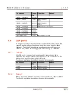
Page 58: ...g distributed realtime control with a high level of security The DCAN interfaces implement the CAN protocol version 2 0 part A B and supports bit rates up to 1 Mbit s 7 6 1 DCAN0 DCAN0 port is connect...

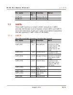
Page 59: ...owing table describes the interface signals Pin name Conn Pin Function Note UART0_RXD J1 7 Receive Data Functions as IrDA receive input in IrDA modes and CIR receive input in CIR mode UART0_TXD J1 8 T...

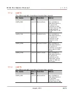
Page 60: ...on pin J2 132 Functions as CIR transmit in CIR mode UART3_RTSn J2 123 Request To Send Also available as alternative function on pin J1 113 Functions as transmit data output in IrDA modes UART3_CTSn J2...

Page 61: ...D SDIO interfaces are available on DIDO module The processor includes 3 MMC SD SDIO Controllers which are compliant with MMC V4 3 Secure Digital Part 1 Physical Layer Specification V2 00 and Secure Di...

Page 62: ...not enabled The following table describes the interface signals Pin name Conn Pin Function Notes SD1_CLK J1 137 Clock output SD1_CMD J1 135 Command output Also available as alternative function on pin...

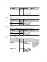
Page 63: ...orts DIDO provides three USB 2 0 ports with integrated PHY USB0 is a OTG 2 0 port USB1 is a Host OTG 2 0 port and USB2 is a 2 0 Host port USB1 can be configured through dedicated mount options USB1 an...

Page 64: ...USBM1 J2 126 7 9 3 USB2 The following table describes the interface signals Pin name Conn Pin Function Notes USBP2 J2 134 Bidirectional data differential signal pair plus minus USBM2 J2 136 7 9 4 Othe...

Page 65: ...P J1 43 Y Position Input TSC_YM J1 45 Y Position Input 7 11 EEPROM One EEPROM is available to provide additional non volatile storage area for user specific usage It is connected to the I2C 3 bus A1 a...

Page 66: ...umn 3 KP_COL4 J1 79 Keypad column 4 KP_COL5 J1 88 Keypad column 5 KP_COL6 J1 85 Keypad column 6 KP_COL7 J1 106 Keypad column 7 7 13 PCI Express The device supports connections to PCIe compliant device...

Page 67: ...pins are not used as optional SATA these pins can be left unconnected SERDES_CLKN J2 38 7 14 SPI buses Three SPI channels are available on DIDO Each port has a maximum supported frequency of 48 MHz an...

Page 68: ...chip selects SPI 2 _SCS 1 J2 45 SPI 2 _SCS 0 J2 50 SPI 2 _D 1 J1 78 J2 47 SPI Data I O Can be configured as either MISO or MOSI SPI 2 _D 0 J1 80 J2 21 J2 42 7 14 3 SPI3 SPI3 provides 3 chip select sig...

Page 69: ...O buffers A third I2C channel I2C0 is used for the internal connection between CPU and PMIC please refer to Section 5 2 7 15 1 I2C2 The following table describes the interface signals Connector Pin P...

Page 70: ...rovides a Serial ATA SATA 3 0 Gbps controller with integrated PHY which supports all SATA power management features port multiplier with command based switching and activity LEDs It also provides hard...

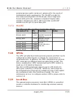
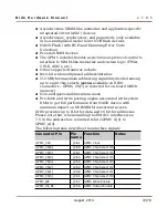
Page 71: ...MCA 2 _AXR 2 J2 90 MCA 2 _AXR 3 J2 92 7 18 GPIOs The GPIO peripheral provides general purpose pins that can be configured as either inputs or outputs for connections to external devices In addition t...

Page 72: ...served for on board NAND memory Non multiplexed address data mode Pre fetch and write posting engine associated with system DMA to get full performance from NAND device with minimum impact on NOR SRAM...

Page 73: ...MC_WAIT 1 J2 61 GPMC Wait 1 GPMC_A 15 J1 86 GPMC Address lines GPMC_A 14 J1 112 J2 39 GPMC_A 13 J1 106 J2 34 GPMC_A 12 J1 87 GPMC_A 11 J1 77 GPMC_A 10 J1 85 GPMC_A 9 J1 110 GPMC_A 8 J1 79 GPMC_A 7 J1...

Page 74: ...D i d o H a r d w a r e M a n u a l v 1 0 5 Connector Pin Pin name Function Notes GPMC_D 1 J2 4 GPMC_D 0 J2 5 August 2014 74 78...

Page 75: ...r application upon DIDO module because in most cases this would lead to an over sized power supply unit Several configurations have been tested in order to provide figures that are measured on real wo...

Page 76: ...ge Shunt Voltage Current Power Consumpion Linux prompt M3 unloaded 3266 mV 8 mV 779 mA 2550 mW Linux prompt M3 loaded 3261 mV 10 mV 1040 mA 3400 mW cpuBurnA8 M3 Loaded 3258 mV 12 mV 1235 mA 3900 mW de...

Page 77: ...CortexA8 s for further information Please note that shunt voltage value is rounded Please note that although the NAON module has been used during these tests usage of the DIDO module would lead to com...

Page 78: ...ollowing documents available on DAVE Embedded Systems Developers Wiki Document Location Integration Guide http wiki dave eu index php Inte gration_guide_ 28Dido 29 Carrier board design guidelines http...

Page 79: ...Mouser Electronics Authorized Distributor Click to View Pricing Inventory Delivery Lifecycle Information DAVE Embedded Systems DOH5210D...

Reviews: