background image


RD-19230EX-300 / RD-19240EX-300

User’s Guide 

Evaluation Board for the 

RD-19230 & RD-19240 

Monolithic Tracking Resolver to 

Digital Converters 

MN-19230EX-001 


The information in this User’s Guide is believed to be accurate; however, no 

responsibility is assumed by Data Device Corporation for its use, and no license or rights 

are granted by implication or otherwise in connection therewith. 

Specifications are subject to change without notice. 


Please visit our web site at 

www.ddc-web.com

 for the latest information. 


105 Wilbur Place, Bohemia, New York 11716-2426 


For Technical Support - 1-800-DDC-5757 ext. 7771 
Headquarters - Tel: 1-800-DDC-5757, Fax: (631) 567-7358 
Southeast - Tel: (703) 450-7900, Fax:  (703) 450-6610 
West Coast - Tel: (714) 895-9777, Fax:  (714) 895-4988 
United Kingdom - Tel: +44-(0)1635-811140, Fax: +44-(0)1635-32264 
Ireland - Tel: +353-21-341065, Fax: +353-21-341568 
France - Tel: +33-(0)1-41-16-3424, Fax: +33-(0)1-41-16-3425 
Germany - Tel: +49-(0)89-150012-11, Fax: +49-(0)89-150012-22 
Japan - Tel: +81-(0)3-3814-7688, Fax: +81-(0)3-3814-7689 
World Wide Web – 

http://www.ddc-web.com


DATA DEVICE CORPORATION
REGISTERED TO ISO 9001:2000

FILE NO. A5976

R

E

G

IS

T ERED

FI

R

M

®

U

All rights reserved.  No part of this User’s Guide may 

be reproduced or transmitted in any form or by any 

means, electronic, mechanical, photocopying, 

recording, or otherwise, without the prior written 

permission of Data Device Corporation. 

Rev E, August, 2006 

© 2002 Data Device Corp. 

Summary of Contents for RD-19230EX-300

Page 1: ...771 Headquarters Tel 1 800 DDC 5757 Fax 631 567 7358 Southeast Tel 703 450 7900 Fax 703 450 6610 West Coast Tel 714 895 9777 Fax 714 895 4988 United Kingdom Tel 44 0 1635 811140 Fax 44 0 1635 32264 Ir...

Page 2: ...d manual to add RD 19240EX 300 information Updated RD 19230EX 300 RD 19240EX 300 Schematic page 16 D 01 2006 1 3 4 6 8 9 Updated Introduction page Figure 2 Table 1 Quick Reference Guide Figure 4 Added...

Page 3: ...t P3 connector 8 Using the P3 expansion slot to control the digital inputs 9 Using P3 to Read Data 9 Digital Input Control 11 SW1 Refer to Figure 2 location 12 11 TB2 Refer to Figure 2 location 14 11...

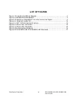
Page 4: ...Vrms Line to Line Signal 4 Figure 4 Component Carrier S3 10 Figure 5 LVDT 16 Pin Component Carriers 14 Figure 6 3 Wire LVDT Connection 15 Figure 7 2 Wire LVDT Connection 15 Figure 8 Mechanical Specifi...

Page 5: ...2 LED Indicators 4 Table 3 Detailed Guide 7 Table 4 Digital Input Control 11 Table 5 Reference Voltage Scaling 12 Table 6 Signal Input Configuration 12 Table 7 LVDT Mode Configuration 13 Data Device C...

Page 6: ...t Numbers Courier New is used to indicate code examples Indicates user entered text or commands Symbols and Icons The Idea Tip icon will be used to identify a handy bit of supplementary information th...

Page 7: ...e damaged by Electrical Static Discharge ESD physical shock or improper power surges and that precautions are taken to avoid electrocution NEVER insert or remove card with power turned on Ensure that...

Page 8: ......

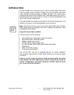
Page 9: ...n with the RD 19230 and RD 19240 data sheets and application manual for detailed specifications setup and application information Support documentation available This board ships with the following RD...

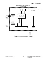
Page 10: ...Board RD 19230FX 300 or RD 19240LS 200 B W 1 B W 2 P S Config Reference Input Configuration Digital Input Configuration Digital Output LEDs Bits 1 thru 16 BIT LED Optional Digital Outputs Bits 1 16 Op...

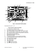
Page 11: ...8 R29 P4 16 Figure 2 Illustrated Parts Breakdown Board dimensions are 2 5 x 3 5 Figure location number descriptions 1 P1 Input power to evaluation board 2 P2 Signal reference input to evaluation card...

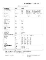
Page 12: ...5V 150ma min 5V 150ma min Signal Input 11 8 Vrms Resolver 11 8 Vrms Resolver Reference Input 2 26 Vrms 2 26 Vrms Reference Frequency 1 5 kHZ 1 5 kHZ Resolution 16 Bit 14 Bit Bandwidth 130HZ 130HZ Trac...

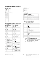
Page 13: ...control requires SW1 2 off 13 Shift P3 control requires SW1 1 off 28 ENL P3 control requires SW1 8 off 14 U B 29 A LSB 1 15 Cb Z1 30 AquadB P3 control requires SW1 3 off P4 Test Points Vel Gnd E S1 S...

Page 14: ...ion See Figure 2 Factory Preset Jumper In Socket Function J1 5V only mode VDDP J2 5V only mode VSSP J3 Up Dn SW1 7 Switch Active J4 Up Dn 5V pull down J5 D1 SW1 5 Switch Active J6 D1 5V pull down J7 D...

Page 15: ...Zin each line to gnd Resolver Zin single ended Zin differential DDC 55688 2V Resolver Zin single ended Zin differential Ohms Ohms Ohms Ohms Ohms Ohms Ohms Ohms Ohms Ohms 52k 35k 70k 140k 195k 130k 26...

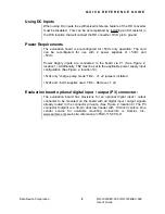
Page 16: ...nnected to the board via P1 See Figure 2 location 1 Additionally TB2 must be set to the applicable power supply input configuration See Figure 2 location 14 5vdc only charge pump mode TB2 J1 J2 jumper...

Page 17: ...controls for UP DN pre charge function resolution control SW1 switches can override some P3 functions and should be in the off position Using P3 to Read Data When using P3 to read bits 1 thru 16 the...

Page 18: ...z For other frequency ranges see table 3 carrier frequency range for instructions to adjust R28 R29 R clock and R set parallel resistors The preset velocity resistor R9 is 357k which will result in a...

Page 19: ...tion 14 Digital inputs DO D1 Up Dn are set to 5vdc using a combination of TB2 jumper settings to disable the appropriate SW1 and apply 5vdc to the specific digital input See table 4 for details Exampl...

Page 20: ...the three 16 pin Dip thin film networks which come with the board The socket insertion location will determine the input type See Table 6 Table 6 Signal Input Configuration Input Type Voltage Thin Fi...

Page 21: ...See Figure 2 location 3 4 and S2 See Figure 2 location 15 To enable LVDT mode 1 Install TB1 J4 J5 2 Remove TB1 J6 J7 J8 3 Remove TB2 J5 J7 4 Set SW1 and TB2 as indicated in table 7 to obtain the desi...

Page 22: ...Q U I C K R E F E R E N C E G U I D E Install in S1 A Install in S1 B Install in S2 Figure 5 LVDT 16 Pin Component Carriers Data Device Corporation RD 19230EX 300 RD 19240EX 300 User s Guide 14...

Page 23: ...Q U I C K R E F E R E N C E G U I D E Figure 6 3 Wire LVDT Connection Figure 7 2 Wire LVDT Connection Data Device Corporation RD 19230EX 300 RD 19240EX 300 User s Guide 15...

Page 24: ...MECHANICAL SPECIFICATIONS 2 5 X 3 5 Board sits on standoffs Figure 8 Mechanical Specifications Data Device Corporation 16 RD 19230EX 300 RD 19240EX 300 User s Guide...

Page 25: ...B INHB ENMB ENLB D0 D1 UPB_DN SHIFT 10 9 8 7 6 5 4 3 2 1 11 12 13 14 15 16 17 18 19 20 SW1 DIGITAL INPUT SWITCHES DGND BIT DGND 2N2907 LED17 R27 750 OHMS LED16 LED15 LED14 LED13 LED12 LED11 LED10 LED9...

Reviews: