background image

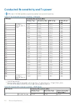
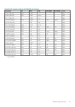
Table 48. Conducted Rx (receive) sensitivity - UMTS bands (continued)

UMTS bands

Conducted Rx sensitivity (dBm)

Primary (Typ)

Secondary (Typ)

Primary/secondary

(Worst case)

a

B2

–111.2

–110.4

–104.7

B4

–110.1

–110.6

–106.7

B5

–111.4

–113.5

–104.7

B6

–111.2

–113.5

–106.7

B8

–111.4

–113.4

–103.7

B9

–110.1

–111.3

–105.7

B19

–111.1

–113.4

–106.7

a.

Per 3GPP specification.

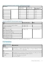
Table 49. Conducted Tx (transmit) power tolerances  

Bands

Conducted Tx power

Notes

LTE

LTE bands 1,2,3,4,5,8,9,12,13,18,19,20,26,28,66

+23 dBm ± 1 dB

-

LTE bands 7,41,42

a

,43

a

,48

a

+22 dBm ± 1 dB

-

UMTS

Band 1 (IMT 2100 12.2 kbps)

+23 dBm ± 1 dB

Connectorized (Class 3)

Band 2 (UMTS 1900 12.2 kbps)

Band 4 (AWS 1700/2100 12.2 kbps)

Band 5 (UMTS 850 12.2 kbps) Band 6 (UMTS 800 12.2 kbps)

Band 8 (UMTS 900 12.2 kbps)

Band 9 (UMTS 1700 12.2 kbps)

Band 19 (UMTS 800 12.2 kbps)

a.

B42/B43/B48 disabled as of publication date, support pending regulatory approval.

5G features

Table 50. 5G features 

Feature

Implementation

General

Data throughput

DL 3.88 Gbps (max. theoretical: 4.14 Gbps) at EN-DC: DC_3C-1A-7C-n78A with LTE 5CA 4x4
MIMO (20 Layers) + Sub6G 4x4 MIMO UL 632 Mbps (max theoretical: 660 Mbps) at (EN-DC:
DC_7C-n78A with LTE UL CA + Sub6G SISO)

5G

Bands

FR1 (Sub 6G): FDD: n1, n2, n3, n5, n7, n8, n12, n20, n28, n66, n71 TDD: n38, n41, n77, n78, n79

Band combinations

For supported E-UTRAN New Radio Dual Connectivity (EN-DC)

4x4 MIMO

n1, n2, n3, n7, n66, n38, n41, n77, n78, n79

DSS

n1, n3, n5, n28, n66, n71

Wireless Specifications

71

Summary of Contents for EGW-5200

Page 1: ...Dell EMC Edge Gateway 5200 User s Guide January 2022 Rev A01 ...

Page 2: ...ential damage to hardware or loss of data and tells you how to avoid the problem WARNING A WARNING indicates a potential for property damage personal injury or death 2022 Dell Inc or its subsidiaries All rights reserved Dell EMC and other trademarks are trademarks of Dell Inc or its subsidiaries Other trademarks may be trademarks of their respective owners ...

Page 3: ...nector 15 DVI D connector 16 VGA connector 17 USB 2 0 ports 17 USB 3 1 ports 17 Gigabit Ethernet ports 17 DC power input 19 COM port connectors 19 Remote power button connector 20 Internal I O connectors 21 Mainboard connector locations 21 USB 2 0 connector 22 Mini PCIe connector 22 SATA connector 22 Clear CMOS jumper 23 Extended PWR RESET header 23 USIM slot 23 Antenna connectors 24 Chapter 4 Get...

Page 4: ...rk Stack Configuration 48 Chipset 49 System Agent SA Configuration 50 PCH IO Configuration 54 Security 58 Secure Boot 59 Media Sanitization Configuration 61 Boot 62 Save and Exit 64 Event logs 65 Change Smbios Event Settings 66 View Smbios Event Log 67 Appendix C Wireless Specifications 68 Wireless frequencies 68 Conducted Rx sensitivity and Tx power 70 5G features 71 Antenna interface specificati...

Page 5: ...2x DDR4 SO DIMM socket supporting up to 32 GB DDR4 per socket for a total of 64 GB 2x DisplayPort 1x DVI D and 1x VGA supporting three independent displays 6x external USB ports 2x USB 3 1 Gen 2 1x USB 3 1 Gen 1 3x USB 2 0 one internal USB 2 0 port Three Intel GbE LAN ports Built in 8 ch DI and 8 ch DO two software programmable RS 232 422 485 two RS 232 ports Built in wide range 12 V DC to 24 V DC...

Page 6: ...C adapters 180 W for EGW 5200 system 60 W for GbE PoE module 4G module 5G module uFM modules 2x Isolated COM RS 422 485 2x Isolated COM RS 232 2x GbE with PoE Out 2x Isolated LAN 2x Isolated Canbus Isolated DI O 6 Introduction ...

Page 7: ...ce Display 2x DP DVI D VGA three independent displays Ethernet 3x Intel GbE 2x i210 i219LM PHY iAMT supported on i5 and i7 CPUs Serial ports COM1 2 RS 232 422 485 COM3 4 RS 232 DI O 8 ch DI and 8 ch DO USB 6x external USB ports 2x USB 3 1 Gen 2 1x USB 3 1 Gen 1 3x USB 2 0 one internal USB 2 0 port Audio Line out mic in Mini PCIe 1x full size USB 2 0 PCIe used for WiFi by default M 2 1x socket 2 ke...

Page 8: ...imum operating temperature of the EGW 5200 is 60 C 140 F Do not exceed this maximum temperature while operating the EGW 5200 inside an enclosure Internal heating of the device electronics other electronics and the lack of ventilation inside an enclosure can cause the operating temperature of the EGW 5200 to be greater than the outside ambient temperature Continuous operation at temperatures greate...

Page 9: ... HDA Audio Cable SPI BIOS GPIO 8DI 8DO Wafer DI DO DB26 Cable LPC bus TPM 2 0 SIO NCT6106D Cable 2x RS232 2x RS232 422 485 DB9 CN M 2 Conn 2280 3042 size PCIe i219 PCIe i210 PCIe i210 GLAN RJ45 CN GLAN RJ45 CN GLAN 2x PCIe or SATA USB2 USB3 Mini PCIe Full size 1x PCIe USB2 0 2x SATA Conn 1x 2 5 storage 2x SATA Cable 2x 2 5 storage External port Internal port Intel Coffee Lake S Processor DP to DVI...

Page 10: ...llation of a uFM module requires removal of COM3 and COM4 ports With the exception of the 8x DI O module it also requires removal of WiFi Display options With computing and graphic performance enhancement from its 9th Generation Intel processors the EGW 5200 controller can support three independent displays with the following configurations Table 3 Maximum available resolution display configuratio...

Page 11: ...Mechanical dimensions B 225 00 mm 5 2 mm 7 2 mm 20 2 mm R4 0 16 9 mm 5 2 mm 89 50 mm 179 00 mm 212 80 mm Figure 2 EGW 5200 top view including wall mount brackets Specifications 11 ...

Page 12: ...re 3 EGW 5200 side view including wall mount brackets 211 mm 238 mm 86 mm 88 mm Figure 4 EGW 5200 front view including wall mount brackets 136 2 110 9 2 6 0 Figure 5 WiFi antenna dimensions in mm 12 Specifications ...

Page 13: ... Front panel I O legend Letter Description Letter Description A DC Power Input I Extend Power Button B DisplayPort x2 J Power C DVI D K Reset D VGA L Audio mic phones speaker E 3x USB 3 1 Type A Gen2 red ports 1 and 2 Gen1 blue port 4 M Digital Input Output F 3x Gigabit Ethernet N 2x COM ports 232 485 capable G 3x USB 2 0 Type A black ports 3 5 and 6 O uFM I O default with 2x COM ports H LED Indic...

Page 14: ... Diagnostic DG Green When illuminated continuously indicates no physical storage is connected If blinking indicates no memory is installed on either SO DIMM socket U1 U2 U3 Green Behavior can be adjusted using onboard GPIO Reset button The reset button executes a hard reset for the EGW 5200 DisplayPort connectors Two DisplayPort connectors on the front panel can connect to VGA DVI HDMI and Display...

Page 15: ... N channel MOSFET driver with internal pull high of 200 Ω resistance Source sink current for all channels 24 mA VOH 2 4 V to 5 V VOL 0 V to 0 5 V Figure 8 Digital I O connector pin locations Table 7 Digital I O connector pin definitions Pin Signal Pin Signal Pin Signal Pin Signal 1 DI0 8 DI7 15 N C 22 DO3 2 DI1 9 GND 16 N C 23 DO4 3 DI2 10 N C 17 N C 24 DO5 4 DI3 11 N C 18 GND 25 DO6 5 DI4 12 N C ...

Page 16: ...ector pin locations Table 8 DVI D connector pin definitions Pin Signal Pin Signal Pin Signal 1 DVIdata 2 10 DVIdata 1 19 GND 2 DVIdata 2 11 GND 20 N C 3 GND 12 N C 21 N C 4 N C 13 N C 22 GND 5 N C 14 5 V 23 DVI clock 6 DVIDC clock 15 GND 24 DVI clock 7 DVIDC data 16 Hot plug detect C5 GND 8 N C 17 DVIdata 0 9 DVIdata 1 18 DVIdata 0 16 System Layout ...

Page 17: ... including USB flash drive USB external hard drive USB floppy USB CD ROM and others The boot priority and boot device can be configured in BIOS USB 3 1 ports The EGW 5200 provides two USB 3 1 Gen2 red ports and one USB 3 1 Gen1 blue port all supporting Type A USB 3 1 connection on the front panel These ports have a 900 mA power capacity All USB 3 1 ports are compatible with SuperSpeed Gen2 high sp...

Page 18: ... Ethernet port and LEDs Table 10 Ethernet port pin definitions Pin 10BASE T 100BASE TX 1000BASE T 1 TX LAN_TX0 2 TX LAN_TX0 3 RX LAN_TX1 4 LAN_TX2 5 LAN_TX2 6 RX LAN_TX1 7 LAN_TX3 8 LAN_TX3 Table 11 Active Link LED indicators LED Color Status Description Yellow OFF Ethernet port is disconnected ON Ethernet port is connected with no activity Flashing Ethernet port is connected and active Table 12 S...

Page 19: ...power ensure the voltage and polarity provided are compatible with the DC input Use an approved power source as certified by IEC or UL Improper input voltage and or polarity can be responsible for system damage COM port connectors The EGW 5200 provides four COM ports through D sub 9 pin connectors The COM1 and COM2 ports support RS 232 422 485 modes by BIOS setting while COM3 and COM4 are located ...

Page 20: ...r button with pin definitions as detailed in the following figure and table These pins are normally open NO Figure 16 Remote power button header pin locations Manufacturer Alex Manufacturer part number 9566 02 G Dimensions Distance from center of pin 1 to center of pin 2 0 100 2 54 mm Width of connector 0 199 5 05 mm Terminal 9588T Brass 9588TP Phosphor bronze Table 16 Remote power button header p...

Page 21: ...Internal I O connectors Mainboard connector locations Figure 17 Mainboard connectors System Layout 21 ...

Page 22: ...c in and line out O Wafer for COM x4 P Wafer for I2C sensor Q Internal power button R PCIe x16 slot for PCIe and BP power S RTC battery T Board to Board for AFM board U PWR for AFM MXM carrier board 12 V V Clear CMOS Jumper USB 2 0 connector One USB 2 0 Type A connector is provided on the mainboard for internal USB dongle with another on the backplane board Mini PCIe connector The internal Mini PC...

Page 23: ...replace to pins 2 and 3 default Figure 18 Clear CMOS jumper setting Extended PWR RESET header An internal header is provided for the Power and Reset buttons with pin definitions as shown Figure 19 PWR RESET header pin locations Table 18 PWR RESET header pin definitions Pin Signal 1 PWR_BTN L 2 GND 3 GND 4 RESET_BTN L USIM slot Two physical USIM card slots are located on the right hand side of the ...

Page 24: ...cation ANT1 4G Main 5G LTE TX RX Right side panel ANT2 WiFi Back panel ANT3 WiFi Bluetooth Back panel ANT4 5G LTE RX GNSS Back panel ANT5 5G LTE RX 4G GNSS Back panel ANT6 4G Aux 5G LTE TX RX Back panel ANT7 Unused Front panel ANT8 Unused Front panel 24 System Layout ...

Page 25: ...t up the operating system Mount the device Expansion module installation Attach the WiFi antennas Steps 1 Locate the antennas that are included in the Accessory Box and find the antenna connections on the back panel of the device as shown in the following figure Figure 21 Antenna connections ANT2 and ANT3 2 Attach one antenna to the ANT2 for WiFi 3 Attach the other antenna to the ANT3 for WiFi and...

Page 26: ...utlined in the red rectangle in the following figure and secure it to the chassis using the captive screws Connect the chassis ground screw as shown in the red circle to an appropriate grounding point Figure 24 DC power input Table 20 DC power input pin definitions Pin Signal 1 V DC_IN 2 V DGND 3 Connect a DC power source to the inputs of the DC power connector making sure to use the correct input...

Page 27: ...Mount the device Steps 1 Install the wall mount brackets To attach the wall mount brackets to the chassis remove the outer six M4 6 mm screws that secure the bottom panel to the chassis and then use the same screws to attach the brackets through the mounting holes as indicated by the red circles in the following figure Figure 25 Wall mount bracket installation 2 Mount the device to a wall using th...

Page 28: ...satile expansion kit solutions including isolated 2x COM RS 232 or RS 422 485 2x GbE with PoE 2x GbE LAN 2x Canbus 8x DI O 4G and 5G modules For information about safety and proper installation go to the EGW 5200 page of the Dell Technologies Support and click the Documentation tab 28 Getting Started ...

Page 29: ...only Actual power consumption will vary with different attached devices and operating system Table 22 Power consumption System Power off System idle Processor full load System full load Recommended power supply EGW 5200 Intel Core i7 3 6 W 24 W 65 W 97 W 120 W EGW 5200 Intel Core i5 3 7 W 22 W 64 W 94 W 120 W EGW 5200 Intel Core i3 3 8 W 22 W 56 W 85 W 120 W NOTE Sufficient power supply for the en...

Page 30: ...d the POST Power On Self Test message is displayed The EGW 5200 controller supports a one time Boot Menu allowing selection of a boot device Enter the Boot Menu by selecting F7 at POST Note the following BIOS setup details The default password is service tag include exclamation point BIOS options listed are for reference only Different configurations can affect BIOS behavior Displayed material may...

Page 31: ...Main Figure 27 BIOS screen Main tab BIOS Setup 31 ...

Page 32: ...Advanced Figure 28 BIOS screen Advanced tab 32 BIOS Setup ...

Page 33: ...CPU Configuration Figure 29 CPU Configuration top of screen BIOS Setup 33 ...

Page 34: ...lization Technology Intel Trusted Execution Technology Disabled Enabled Enables utilization of additional hardware capabilities provided by Intel Trusted Execution Technology Intel R SpeedStep tm Disabled Enabled Allows more than two frequency ranges to be supported Intel R Speed Shift Technology Disabled Enabled Enable disable Intel Speed Shift Technology support Enabling will expose the CPPC v2 ...

Page 35: ...bled Enabled Enable disable Power Limit 1 override If this option is disabled BIOS will program the default values for Power Limit 1 and Power Limit 1 Time Window Power Limit 1 0 Power Limit 1 in milliwatts BIOS will round to the nearest 1 8 W when programming 0 no custom override For 12 50 W enter 12500 Overclocking SKU Value must be between Max and Min Power Limits specified by PACKAGE_POWER_SKU...

Page 36: ...nable or disable system wake on alarm event Select FixedTime system will wake on the hr min sec specified Select DynamicTime system will wake on the current time increase minute s Wake up hour 0 Range 0 23 hr Wake up minute 0 Range 0 59 min Wake up second 0 Range 0 59 sec Wake up minute increase 1 Range 1 5 min Ring Wake Disabled Enabled Disable enable RI ping for Wake On Ring function PCH PME sig...

Page 37: ... capability Serial Console Redirection Figure 32 Serial Console Redirection Table 25 Serial Console Redirection Parameter Settings Description COM1 Console Redirection Disabled Enabled Console Redirection Enable or Disable COM Pci Bus0 Dev22 Func3 Console Redirection Disabled Enabled Console Redirection Enable or Disable BIOS Setup 37 ...

Page 38: ...eed The speed must be matched on the other side Long or noisy lines may require lower speeds Data Bits 7 8 Data Bits Parity None Even Odd Mark Space A parity bit can be sent with the data bits to detect some transmission errors Even parity bit is 0 if the number of 1s in the data bits is even Odd parity bit is 0 if number of 1s in the data bits is odd Mark parity bit is always 1 Space Parity bit i...

Page 39: ... Enable VT UTF8 Combination Key Support for ANSI VT100 terminals Recorder Mode Disabled Enabled With this mode enabled only text is sent This is to capture terminal data Resolution 100x31 Disabled Enabled Enables or disables extended terminal resolution Putty KeyPad VT100 LINUX XTERMR6 SCO ESCN VT400 Select FunctionKey and KeyPad on Putty Figure 34 Console Redirection COM Pci Bus0 Dev22 Func3 Tabl...

Page 40: ...p bits indicate the end of a serial data packet a start bit indicates the beginning The standard setting is one stop bit Communication with slow devices may require more than one stop bit Flow Control None Hardware RTS CTS Flow control can prevent data loss from buffer overflow When sending data if the receiving buffers are full a stop signal can be sent to stop the data flow Once the buffers are ...

Page 41: ... time out 1 sec 5 sec 10 sec 20 sec The time out value for Control Bulk and Interrupt transfers Device reset time out 10 sec 20 sec 30 sec 40 sec USB mass storage device start unit command time out Device power up delay Auto Manual Maximum time that the device takes to properly report itself to the host controller Auto uses the default value For a root port it is 100 ms and for a hub port the dela...

Page 42: ...e SHA 1 PCR Bank SHA256 PCR Bank Disabled Enabled Enable or disable SHA256 PCR Bank Pending operation None TPM Clear Schedule an operation for the security device The computer reboots during restart to change the state of the security device Platform Hierarchy Disabled Enabled Enable or disable Platform Hierarchy Storage Hierarchy Disabled Enabled Enable or disable Storage Hierarchy Endorsement Hi...

Page 43: ...sables Platform Hierarchy randomization Do not enable in production platforms This is for development testing Override ChangePlatformAuth ELINK for production platforms supporting TXT Device Select TPM 1 2 TPM 2 0 Auto TPM 1 2 restricts support to TPM 1 2 devices TPM 2 0 restricts support to TPM 2 0 devices Auto supports both with the default set to TPM 2 0 devices If not found TPM 1 2 devices are...

Page 44: ...isabled Enabled OEMFLag Bit 1 Enable automatic MEBx hotkey press Onboard Devices Configuration Figure 38 Onboard Devices Configuration Table 31 Onboard Devices Configuration Parameter Settings Description Serial Port Configuration COM1 Device Settings IO 3F8h IRQ 4 COM1 Control RS232 RS422 RS485 Select COM1 mode RS232 RS422 or RS485 COM2 Device Settings IO 2F8h IRQ 3 COM2 Control RS232 RS422 RS485...

Page 45: ...meter Settings Description COM4 Device Settings IO 2E8h IRQ 7 Lan Port Configuration LAN 1 Intel I219 Enabled Disabled LAN 2 Intel I210IT Enabled Disabled LAN 3 Intel I210IT Enabled Disabled NCT6106D HW Monitor Figure 39 NCT6106D HW Monitor BIOS Setup 45 ...

Page 46: ...eter Settings Description BIOS POST Watchdog Disabled Second Mode Minute Mode Disabled Disable WatchDog Timer Second Mode Enable Watchdog Timer in second mode Minute Mode Enable Watchdog Timer in minute mode BIOS Watchdog Timer 45 Set Watchdog Timer for BIOS POST process 46 BIOS Setup ...

Page 47: ...NVMe Configuration Figure 41 NVMe Configuration BIOS Setup 47 ...

Page 48: ...ot support is not available Ipv6 PXE Support Disabled Enabled Enable disable IPv6 PXE boot support If disabled IPv6 PXE boot support is not available Ipv6 HTTP Support Disabled Enabled Enable disable IPv6 HTTP boot support If disabled IPv6 HTTP boot support is not available IPSEC Certificate Disabled Enabled Support to enable disable IPSEC certificate for Ikev PXE boot wait time 0 Wait time in sec...

Page 49: ...n Above 4G Decoding Disabled Enabled Enables or disables 64 bit capable devices to be decoded in Above 4G Address Space only if system supports 64 bit PCI decoding PCH digital I O device Disabled Enabled Disable enable ACPI GPIO device support for PCH digital I O and user LED BIOS Setup 49 ...

Page 50: ...System Agent SA Configuration Figure 44 System Agent Configuration Table 35 System Agent Configuration Parameter Settings Description VT d Disabled Enabled VT d capability 50 BIOS Setup ...

Page 51: ...Memory Configuration Figure 45 Memory Configuration BIOS Setup 51 ...

Page 52: ... the setup options GTT Size 2MB 4MB 8MB Select the GTT size Aperture Size 128MB 256MB 512MB 1024MB 2048MB Select the aperture size DVMT Pre Allocated 4M 8M 16M 32M 64M Select DVMT 5 0 pre allocated fixed graphics memory size used by the internal graphics device DVMT Total Gfx Mem 128M 256M MAX Select DVMT 5 0 total graphic memory size used by the internal graphics device 52 BIOS Setup ...

Page 53: ...DMI OPI Configuration Figure 47 DMI OPI Configuration Table 37 DMI OPI Configuration Parameter Settings Description DMI Max Link Speed Auto Gen1 Gen2 Gen3 Set DMI speed Gen1 Gen2 Gen3 BIOS Setup 53 ...

Page 54: ...PCH IO Configuration Figure 48 PCH IO Configuration 54 BIOS Setup ...

Page 55: ...ntel RST Premium With Intel Optane System Acceleration Determines how SATA controller s operate SATA Controller Speed Default Gen1 Gen2 Gen3 Indicates the maximum speed the SATA controller can support SATA HDD 1 Empty SATA HDD 1 Disabled Enabled Enable or disable SATA HDD 2 TS2TSSD452KI A 2048 4GB SATA HDD 2 Disabled Enabled Enable or disable BIOS Setup 55 ...

Page 56: ...Security Configuration Figure 50 Security Configuration 56 BIOS Setup ...

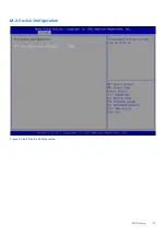
Page 57: ...M 2 Device Configuration Figure 51 M 2 Device Configuration BIOS Setup 57 ...

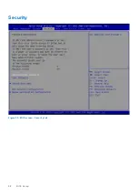
Page 58: ...Security Figure 52 BIOS screen Security tab 58 BIOS Setup ...

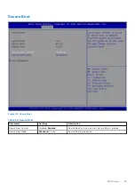
Page 59: ...cure Boot Table 39 Secure Boot Parameter Settings Description Secure Boot Control Disabled Enabled Secure Boot feature is active if Secure Boot is enabled Secure Boot Mode Standard Custom Secure Boot mode options BIOS Setup 59 ...

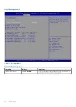
Page 60: ...ey Management Table 40 Key Management Parameter Settings Description Factory Key Provision Disabled Enabled Install factory default Secure Boot keys after the platform is reset and while the system is in setup mode 60 BIOS Setup ...

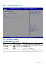
Page 61: ...Purge Clear write zero into HDD or SSD and purge write random pattern inverted random pattern and zeros sequentially Command Type None Sanitize Secure Erase Format Sanitize secure format Password Type User Master Compare user or master password Erase Mode Normal Enhanced Normal Erase mode write vendor specific pattern and Enhanced Erase mode also erase password BIOS Setup 61 ...

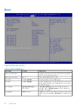
Page 62: ... option Fast Boot Disabled Enabled Enables or disables boot with initialization of a minimal set of devices required to launch active boot option Has no effect on BBS boot options SATA Support Last Boot HDD Only All Sata Devices If Last Boot HDD Only only the last boot HDD device is available in post If All Sata Devices all SATA devices are available in OS and post VGA Support Auto EFI Driver If A...

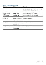
Page 63: ...es are skipped NetWork Stack Driver Support Disabled Enabled If disabled NetWork Stack Driver is skipped Redirection Support Disabled Enabled If disabled the redirection function is disabled Boot Configuration Boot Option 1 Hard Disk USB Key USB CD DVD USB Hard Disk USB Floppy USB Lan CD DVD Network Disabled Sets the system boot order Boot Option 2 Hard Disk USB Key USB CD DVD USB Hard Disk USB Fl...

Page 64: ...Save and Exit Figure 57 BIOS screen Save and Exit tab 64 BIOS Setup ...

Page 65: ...Event logs Figure 58 BIOS screen Event logs tab BIOS Setup 65 ...

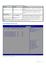
Page 66: ... No Yes Next reset Yes Every reset Choose options for erasing Smbios Event Log Erasing is done prior to any logging activation during reset When Log is Full Do Nothing Erase Immediately Choose options for reactions to a full Smbios Event Log Smbios Event Log Standard Settings Log System Boot Event Disabled Enabled Choose option to enable disable logging of system boot events MECI 1 Multiple Event ...

Page 67: ...nges from 0 to 99 minutes Custom Options Log EFI Status Code Disabled Enabled Enable or disable the logging of EFI Status Codes as OEM reserved type E0 if not already converted to legacy Convert EFI Status Codes to Standard Smbios Type Disabled Enabled Enable or disable the converting of EFI Status Codes to standard Smbios types not all may be translated NOTE All values changed here do not take ef...

Page 68: ...Hz 925 960 MHz B9 1749 9 1784 9 MHz 1844 9 1879 9 MHz B12 699 716 MHz 729 746 MHz B13 777 787 MHz 746 756 MHz B18 815 830 MHz 860 875 MHz B19 830 845 MHz 875 890 MHz B20 832 862 MHz 791 821 MHz B26 814 849 MHz 859 894 MHz B28 703 748 MHz 758 803 MHz B29 n a 717 728 MHz B30 2305 2315 MHz B30 Tx is disabled 2350 2360 MHz B32 n a 1452 1496 MHz B41 2496 2690 MHz TDD B42a 3400 3600 MHz TDD B43a 3600 38...

Page 69: ...icted by the network for some channel assignments in FDD TDD co existence scenarios in order to meet unwanted emissions requirements Clause 6 6 3 2 of 3GPP TS 36 521 1v12 6 0 c B42 B43 B48 disabled as of publication date support pending regulatory approval Table 46 WCDMA frequency bands support Band Frequency Tx Frequency Rx Band 1 1920 1980 MHz 2110 2170 MHz Band 2 1850 1910 MHz 1930 1990 MHz Ban...

Page 70: ...98 5 100 5 102 5 96 3 B20 98 5 101 0 103 5 93 3 B26 99 0 100 5 102 5 93 8 B28 98 5 100 5 102 5 94 8 B29 97 0 101 0 102 5 93 3 B30 97 0 99 0 101 0 95 3 B32 99 5 98 0 101 5 96 3 B41 96 5 98 0 100 5 94 3 B42c 97 0 98 5 101 0 95 0 B43c 97 0 97 5 101 0 95 0 B48c 97 0 98 0 101 0 95 3 B66 97 0 98 0 100 0 95 8 B46 Full RB on downlink BW 20 MHz 96 5 97 0 99 0 88 5 a Per 3GPP specification b Sensitivity val...

Page 71: ... 1900 12 2 kbps Band 4 AWS 1700 2100 12 2 kbps Band 5 UMTS 850 12 2 kbps Band 6 UMTS 800 12 2 kbps Band 8 UMTS 900 12 2 kbps Band 9 UMTS 1700 12 2 kbps Band 19 UMTS 800 12 2 kbps a B42 B43 B48 disabled as of publication date support pending regulatory approval 5G features Table 50 5G features Feature Implementation General Data throughput DL 3 88 Gbps max theoretical 4 14 Gbps at EN DC DC_3C 1A 7C...

Page 72: ...s Compressed mode CM supported according to 3GPP TS25 212 Output power all bands 24 dBm 1 7 3 7 dB Antenna interface specification Measurement conditions ambient temperature 25 C V3V3 3 3 V Typical values RX measured at 10 MHz bandwidth TX 1 RB at max Table 51 RF antenna interface LTE 5G NR Conditions Tx PRx DRx PRX MIMO DRX MIMO Unit LTE 2100 Band 1 23 3 97 97 5 97 5 97 5 dBm LTE 1900 Band 2 23 2...

Page 73: ... 23 8 98 97 96 5 97 dBm LTE 1900 Band 39 23 8 97 98 a a dBm LTE 2500 Band 41 23 4 97 97 97 5 96 5 dBm LTE 3500 Band 42 23 5 98 98 97 97 5 dBm LTE 5200 Band 46 97 5 97 a a dBm LTE 3500 Band 48 21 3 98 98 97 5 97 dBm LTE AWS 3 Band 66 23 4 97 98 98 5 98 dBm LTE 600 Band 71 23 3 99 5 102 a a dBm 5G NR 2100 Band n1 23 7 92 93 93 93 dBm 5G NR 1900 Band n2 23 5 92 92 5 92 92 dBm 5G NR 1800 Band n3 23 3 ...

Page 74: ...ipped with the device and on the associated device before handling operating the device to avoid injury or damage WARNING Risk of explosion if battery is replaced with one of an incorrect type please dispose of used batteries appropriately WARNING Hot surface Do not touch Touching this surface could result in bodily injury To reduce risk allow the surface to cool before touching D 74 Important Saf...

Page 75: ...ona a continuación se mostrará en los dispoitivos que se describen en este documento en conformidad con los requisitos de la Norma Oficial Mexicana NOM Importador Dell Mexico S A de C V AV Paseo de la Reforma No 2620 Piso 11 Col Lomas Altas Mexico DF CP 11950 Modelo EGW 5200 Voltaje de salida 12 24 VDC País de origen Taiwan E Compliance 75 ...

Page 76: ...Any changes or modifications not expressly approved by the party responsible for compliance could void the user s authority to operate this equipment This transmitter must not be co located or operating in conjunction with any other antenna or transmitter Radiation exposure statement This equipment complies with FCC radiation exposure limits set forth for an uncontrolled environment This equipment...

Page 77: ...Dell EMC offers a variety of product return programs and services in several countries to assist equipment owners in recycling their IT products Waste electrical and electronic equipment WEEE directive for recovery recycle and reuse of IT and telecommunications products Dell EMC appliances are labeled in accordance with European Directive 2002 96 EC concerning waste electrical and electronic equip...

Page 78: ...For information on Dell EMC product recycling offerings see the WEEE Recycling instructions on Support For more information contact the Dell EMC Technical Assistance Center 78 Compliance ...

Reviews: