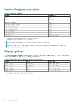
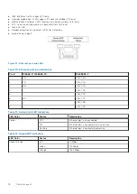
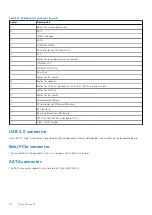
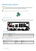
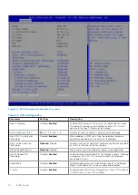
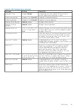

Antenna connectors
Table 19. Antenna connectors
Antenna
Function
Location
ANT1
4G Main
5G/LTE TX/RX
Right-side panel
ANT2
WiFi
Back panel
ANT3
WiFi/Bluetooth
Back panel
ANT4
5G/LTE RX, GNSS
Back panel
ANT5
5G/LTE RX
4G GNSS
Back panel
ANT6
4G Aux
5G/LTE TX/RX
Back panel
ANT7
Unused
Front panel
ANT8
Unused
Front panel
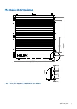
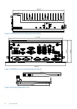
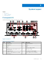
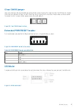
24
System Layout
Summary of Contents for EGW-5200
Page 1: ...Dell EMC Edge Gateway 5200 User s Guide January 2022 Rev A01 ...
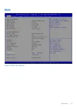
Page 31: ...Main Figure 27 BIOS screen Main tab BIOS Setup 31 ...
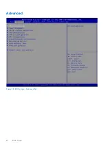
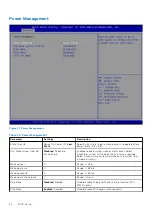
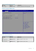
Page 32: ...Advanced Figure 28 BIOS screen Advanced tab 32 BIOS Setup ...
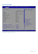
Page 33: ...CPU Configuration Figure 29 CPU Configuration top of screen BIOS Setup 33 ...
Page 47: ...NVMe Configuration Figure 41 NVMe Configuration BIOS Setup 47 ...
Page 51: ...Memory Configuration Figure 45 Memory Configuration BIOS Setup 51 ...
Page 54: ...PCH IO Configuration Figure 48 PCH IO Configuration 54 BIOS Setup ...
Page 56: ...Security Configuration Figure 50 Security Configuration 56 BIOS Setup ...
Page 57: ...M 2 Device Configuration Figure 51 M 2 Device Configuration BIOS Setup 57 ...
Page 58: ...Security Figure 52 BIOS screen Security tab 58 BIOS Setup ...
Page 64: ...Save and Exit Figure 57 BIOS screen Save and Exit tab 64 BIOS Setup ...
Page 65: ...Event logs Figure 58 BIOS screen Event logs tab BIOS Setup 65 ...