background image


LCP-10G3B4EDR


DELTA ELECTRONICS, INC.


13 Revision: 

0B

2008/9/5

www.deltaww.com


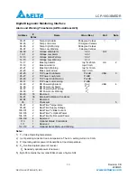
Digital Diagnostic Monitoring Interface 

Alarm and Warning Thresholds (2-Wire Address A2h) 

Address 

Bytes 

Name 

Value (Dec.) 

Unit 

Note

00-01 2 

Temp 

High 

Alarm 

85 degree Celsius


02-03 2 

Temp 

Low 

Alarm 

-10 degree Celsius


04-05 

Temp High Warning 

80 degree Celsius


06-07 

Temp Low Warning 

-5 degree Celsius

 1 

08-09 

Voltage High Alarm 

3.6V


10-11 

Voltage Low Alarm 

3.0V


12-13 

Voltage High Warning 

3.5V


14-15 

Voltage Low Warning 

3.1V


Volt 


16-17 2 

Bias 

High 

Alarm 

   Iop*2+20 mA


18-19 2 

Bias 

Low 

Alarm 

Iop-20 mA


20-21 

Bias High Warning 

   Iop*2+10 mA


22-23 

Bias Low Warning 

Iop-10 mA


mA 2 

24-25 

TX Power High Alarm 

P +3dB


26-27 

TX Power Low Alarm 

P-3dB


28-29 

TX Power High Warning 

P +2dB


30-31 

TX Power Low Warning 

P-2dB


dBm 

32-33 

RX Power High Alarm 

P

0

+2


34-35 

RX Power Low Alarm 

P

S

-2 


36-37 

RX Power High Warning 

P

0

38-39 

RX Power Low Warning 

P

S


dBm 4 

40-45 

16 

Reversed 


56-91 

36 

External Calibration Constants 


92-94 

Reversed 


95 

Checksum 


96-97 

Real Time Temperature 


98-99 

Real Time Supply Voltage 


100-101 

Real Time Tx Bias Current 


102-103 

Real Time Tx Optical Power 


104-105 

Real Time Rx Received Power 


106-109 

Reserved 


110 

Optional Status/ Control Bits 


111 

Reserved 


112-119 

Optional Set of Alarm and Warning 


Notes: 

1) T

C

: Case Operating temperature 

2) I

OP

: Operating current at room temperature. The min. setting current is 0 mA. 

3)  P: Operating optical power of transmitter at room temperature. 
4) P

0

: Overload optical power of receiver 

P

S

: Sensitivity optical power of receiver   

5)  Byte 95 contains the low order 8bits of sum of bytes 0-94 
   

Summary of Contents for 10GBASE-LRM SFP+ Optical Transceiver LCP-10G3B4EDR

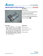
Page 1: ...1W Description The LCP 10G3B4EDR is a hot pluggable 10Gbps small form factor plus transceiver module integrated with the high performance 1310nm FP Laser transmitter high sensitivity linear PD TIA re...

Page 2: ...3 135 3 30 3 465 V Relative Humidity non condensation 5 85 DC Common Mode Voltage VCM 0 3 6 V Low Speed Electrical Characteristics VCC 3 135V to 3 465V Parameter Symbol Min Typ Max Unit Note Total Sup...

Page 3: ...er Symbol Min Typ Max Unit Note Data Rate R 10 3125 Gb s Signaling speed variation from nominal 100 ppm Average Output Power Pavg 6 5 0 5 dBm Wavelength 1260 1355 nm RMS Spectral Width at 1260nm RMS S...

Page 4: ...naling speed nominal TS 10 3125 Gb s Signaling speed variation from nominal 100 ppm Center Wavelength 1260 1355 nm Overload in OMA PO 1 5 dBm Stressed sensitivity in OMA RSO 6 5 dBm 1 Stressed sensiti...

Page 5: ...ial Interface Clock 6 MOD_ABS Module Absent connected to VeeT or VeeR in the module 4 7 LVTTL I RS0 Not Implement 8 LVTTL O RX_LOS Receiver Loss of Signal Indication 2 9 LVTTL I RS1 Not Implement 10 V...

Page 6: ...D_ABS RX_LOS 1 TX_Fault TX_Fault is a module output pin that when High indicates that the module transmitter has detected a fault condition related to laser operation or safety The TX_Fault output pin...

Page 7: ...OD_DEF0 5 SCL SDA SCL is the 2 wire interface clock and SDA is the 2 wire interface data line SCL and SDA are pulled up to a voltage in the range of 3 14V to 3 46V on the host 6 RX_LOS RX_LOS when Hig...

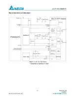
Page 8: ...LCP 10G3B4EDR DELTA ELECTRONICS INC 8 Revision 0B 2008 9 5 www deltaww com Recommend Circuit Schematic...

Page 9: ...EDR DELTA ELECTRONICS INC 9 Revision 0B 2008 9 5 www deltaww com Package Outline Drawing for Metal Housing with Bail de latch Latch Color Identifier Blue Complies with 21 CFR 1040 10 and 1040 11 Made...

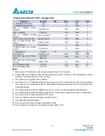
Page 10: ...0 sec 10 RX_LOS negate delay t_los_off 100 sec 11 Notes 1 Rising edge of TX_Disable to fall of output signal below 10 of nominal 2 Falling edge of TX_Disable to rise of output signal above 90 of nomin...

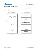
Page 11: ...ormation about the module s present operating conditions 2 wire address 1010000 X A0h 2 wire address 1010001 X A2h 0 0 55 Alarm and Warning Thresholds 56 bytes 95 Serial ID Defined by SFP MSA 96 bytes...

Page 12: ...102 00 17 16 60 05 103 00 18 00 61 1E 104 00 19 16 62 00 105 00 20 44 D 63 CS1 Note 1 106 00 21 45 E 64 01 107 00 22 4C L 65 1A 108 00 23 54 T 66 00 109 00 24 41 A 67 00 110 00 25 20 68 SN Note 2 111...

Page 13: ...P 3dB 28 29 2 TX Power High Warning P 2dB 30 31 2 TX Power Low Warning P 2dB dBm 3 32 33 2 RX Power High Alarm P0 2 34 35 2 RX Power Low Alarm PS 2 36 37 2 RX Power High Warning P0 38 39 2 RX Power L...

Page 14: ...when Tx output power is below low alarm level 113 7 Rx Power High Alarm Set when received power exceeds high alarm level 113 6 Rx Power Low Alarm Set when received power is below low alarm level 113 5...

Page 15: ...act Discharge IEC EN 61000 4 2 Electrostatic Discharge ESD to the Duplex LC Receptacle Air Discharge IEC EN 61000 4 2 Human Body Model HBM MIL STD 883E Method 3015 7 EIA JESD22 A114 Electrostatic Disc...

Reviews: