SPBD-1250A4Q1R
DELTA ELECTRONICS, INC.
4 Revision:
S1
03/12/2007
www.deltaww.com
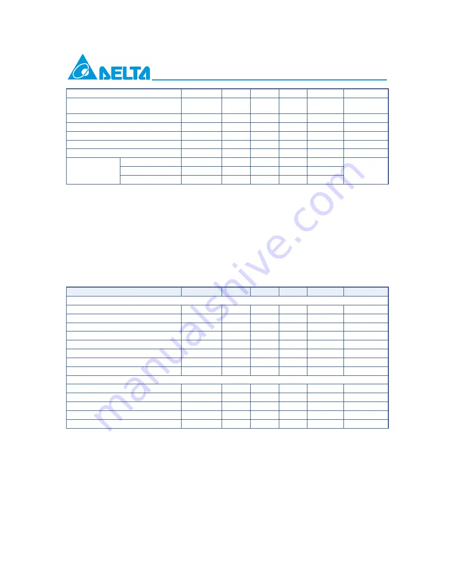
Stressed Receive sensitivity
-15.4
dBm
Stressed Receive sensitivity OMA
44.8
-13.5
uW
dBm
Vertical Eye-closure Penalty
V ECP
2.6
dB
Deterministic Jitter
DJ
170
ps
Total Jitter
TJ
266
ps
Output Data Rise/Fall time
t
r
/t
f
260
ps
Note
(5)
Receiver 3dB upper cutoff frequency
1500
MHz
1260 to 1360nm
-43
dB
1550 to 1560nm
-33
dB
Optical Isolation
from External
Source
1640 to 1665nm
-33
dB
Note (1). Measured with 1490nm, ER=9dB; BER =<10
-12
@PRBS=2
7
-1 NRZ
Note (2). Specified with minimum optical extinction ration of 9dB.
Note (3). When LOS asserted, the data output is Low-level (fixed)
Note (4). When the terminal is viewed from the optical path, the reflection toward the optical path of the
optical signal with a central wavelength of 1480nm to 1500nm transmitted to terminal.
Note (5). These are 20%~80% values
5. Electrical Interface Characteristics
Parameter
Symbol
Min.
Typ.
Max.
Unit
Note
Transmitter
Total Supply Current
I
CC
A
mA
Note
(1)
Differential Data Input Swing
V
DT
500 2400
mV
p-p
Differential line input Impedance
R
IN
80
100
120
Ohm
Transmitter Disable Input-High
V
DISH
2 V
CC
V Note
(2)
Transmitter Disable Input-Low
V
DISL
0 0.8 V
Transmitter Fault Output-High
V
TXFH
2
V
CC
+0.3
V
Transmitter Fault Output-Low
V
TXFL
0 0.8 V
Transmitter Fault Pull up Resistor
R
TX_FAULT
4.7
10
k
Ω
Note
(3)
Receiver
Total Supply Current
I
CC
B
mA
Note
(1)
Differential Data Output Swing
V
DR
400 900
mV
p-p
Note
(4)
LOS Output Voltage-High
V
LOSH
2
V
CC
+0.3
V
LOS Output Voltage-Low
V
LOSL
0 0.8 V
Receiver LOS Load
R
RXLOS
4.7 10 k
Ω
Note
(3)
Note (1). A (TX)+ B (RX) = 300mA
(A: Not include termination circuit; B: using a resister of 150
Ω
between Data-output and ground)
Note (2). There is an internal 4.7 to 10k
Ω
pull-up resistor to VccT.
Note (3). Pull up to V
CC
on host Board.
Note (4). Internally AC coupled with CML output, but requires a 100Ohm differential termination at or
internal to Serializer/ Deserializer.


