background image


SPBD-1250B4Q1R


DELTA ELECTRONICS, INC.


5 Revision: 

S1

03/12/2007

www.deltaww.com


6. Enhanced Digital Diagnostic Interface   

The memory map in the following describes an extension to the memory map defined in SFP MSA. 

The enhanced interface uses the two wire serial bus address 1010001X(A2h) to provide diagnostic 
information about the module’s present operating conditions.   


2 wire address 1010000 X (A0h) 

2 wire address 1010001 X (A2h) 


0 0 

55

Alarm and Warning Thresholds 

(56 bytes) 


95 

Serial ID Defined by SFP MSA 

 (96 bytes) 

56

95

Cal Constants 

(40 bytes) 


96 96

119

Real Time Diagnostic Interface 

 (24 bytes) 


127 

Vender Specific 

 (32 bytes) 

120

127

Vender Specific 


128 128

247

User Writable EEPROM 

(120 bytes) 


255 

Reserved in SFP MSA 

 (128 bytes) 

248

255

Vender Specific 

(8 bytes) 


7. Digital Diagnostic Monitor Accuracy 

Parameter 

Accuracy

Unit

Calibration

Note 

Transceiver Internal Temperature 

±

 3


Internal 

T

C

=-5~+75


Power Supply Internal Voltage 

±

 3% 

V Internal 

V

CC

=3.3V

±

5%


TX Bias Current 

±

 10% 

mA 

Internal 

Specified by nominal bias value

TX Optical Power 

±

 3dB 

dBm

Internal -9 

to 

-3dBm 

RX Optical Power 

±

 3dB 

dBm

Internal -23 

to 

-3dBm 

Note. 

Temperature and Voltage is measured internal to the transceiver.


Summary of Contents for SPBD-1250B4Q1R

Page 1: ...o 1250Mbit sec It is compliant with the Gigabit Ethernet and Fast Ethernet standards as well as the SFP Multisource Agreement MSA The SPBD 1250xxxx transceivers provide with the LC receptacle that is compatible with the industry standard LC connector The transceiver is also compatible with industry standard RFT connector and cage It also includes a LOS Loss Of Signal circuit that provides a TTL lo...

Page 2: ...d on topside of case front center 3 Specification of Transmitter Parameter Symbol Min Typ Max Unit Note Average Launched Power PO 9 6 3 dBm Note 1 Optical Extinction Ratio ER 9 dB Optical Modulation Amplitude OMA 195 7 1 uW dBm Center Wavelength λC 1480 1490 1500 nm DFB Laser Spectrum Width 20dB σ 0 88 nm Side Mode Suppression Ratio SMSR 30 dB Transmitter OFF Output Power POff 45 dBm Optical Rise ...

Page 3: ...Receive sensitivity OMA 44 8 13 5 uW dBm Vertical Eye closure Penalty V ECP 2 6 dB Deterministic Jitter DJ 170 ps Total Jitter TJ 266 ps Output Data Rise Fall time tr tf 260 ps Note 5 Receiver 3dB upper cutoff frequency 1500 MHz Note 1 Measured with 1310nm ER 9dB BER 10 12 PRBS 2 7 1 NRZ Note 2 Specified with minimum optical extinction ration of 9dB Note 3 When LOS asserted the data output is Low ...

Page 4: ...Fault Output Low VTXFL 0 0 8 V Transmitter Fault Pull up Resistor RTX_FAULT 4 7 10 kΩ Note 3 Receiver Total Supply Current ICC B mA Note 1 Differential Data Output Swing VDR 400 900 mVp p Note 4 LOS Output Voltage High VLOSH 2 VCC 0 3 V LOS Output Voltage Low VLOSL 0 0 8 V Receiver LOS Load RRXLOS 4 7 10 kΩ Note 3 Note 1 A TX B RX 300mA A Not include termination circuit B using a resister of 150Ω ...

Page 5: ... ID Defined by SFP MSA 96 bytes 56 95 Cal Constants 40 bytes 96 96 119 Real Time Diagnostic Interface 24 bytes 127 Vender Specific 32 bytes 120 127 Vender Specific 128 128 247 User Writable EEPROM 120 bytes 255 Reserved in SFP MSA 128 bytes 248 255 Vender Specific 8 bytes 7 Digital Diagnostic Monitor Accuracy Parameter Accuracy Unit Calibration Note Transceiver Internal Temperature 3 Internal TC 5...

Page 6: ... MOD DEF1 Module Definition 1 3 Note 4 2 wire serial ID interface 6 MOD DEF0 Module Definition 0 3 Note 4 Grounded in Module 7 Rate Select Not Connect 3 Function not available 8 LOS Loss of Signal 3 Note 5 9 VeeR Receiver Ground 1 10 VeeR Receiver Ground 1 11 VeeR Receiver Ground 1 12 RD Inv Received Data Out 3 Note 6 13 RD Received Data Out 3 Note 6 14 VeeR Receiver Ground 1 15 VccR Receiver Powe...

Page 7: ...ed up with a 4 7K 10KΩ resistor Pull up voltage between 2 0V and VccR 0 3V When high this output indicates the received optical power is below the worst case receiver sensitivity Low indicates normal operation In the low state the output will be pulled to less than 0 8V 6 RD These are the differential receiver outputs They are AC coupled 100Ω differential lines which should be terminated with 100Ω...

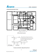
Page 8: ...rotocol IC PLD PAL Mod_def 2 Mod_def 1 Mod_def 0 3 3V 3 3V DELTA SFP Module Preamp Tx_Disable Quantizer Tx_Fault TD TD VeeT RD RD Rx_LOS VeeR Tx_Disable Tx_Fault Rx_LOS RES1 4 7k to 10k Ohms VccT VccR Laser Driver Depands on SerDes IC used EEPROM SFP Host Board Schematic Recommended Host Board Supply Filtering Network Design criterion of the capacitor used is the resonant frequency and its value m...

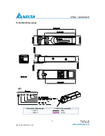
Page 9: ... S1 03 12 2007 www deltaww com 10 Outline Dimensions Transmitter Wavelength Latch Color Identifier 1310nm Black 1490nm Violet Week 52Weeks Year 1月2日 01 Class 1 Laser Product 1040 10 and 1040 11 Made in x Complies with 21 CFR FS XXXX nm Tx Rx XXXX nm ...

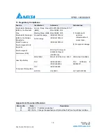
Page 10: ...0 4 2 Radio Frequency Electromagnetic Field Immunity IEC EN 61000 4 3 Electromagnetic Interference EMI FCC Part 15 Class B EN 55022 Class B CISPR 22A 1 Satisfied with electrical characteristics of product spec 2 No physical damage Laser Eye Safety FDA CDRH TUV FDA 21CFR 1040 10 1040 11 IEC EN 60825 1 IEC EN 60825 2 CDRH File 0420993 TUV Certificate R50032471 Component Recognition TUV UL CSA IEC EN...

Reviews: