
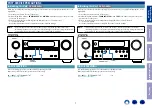
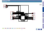

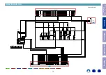
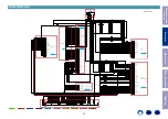
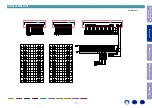
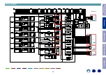
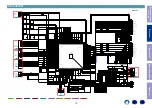
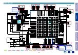
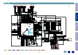

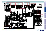
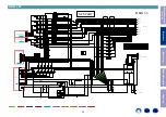
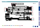
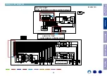
SCH09 ADV8003 DDR
ANALOG AUDIO
DIGITAL AUDIO
TMDS SIGNAL
ANALOG VIDEO
GND LINE
POWER- LINE
POWER+ LINE
DIGITAL VIDEO
STBY POWER
HDMI
DGND
DGND
DGND
DGND
DGND
DGND
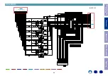
DDR
1
DDR
1
DDR
1
DR
_T
X
D
Q
S
1
DDR
1
DR
_T
X
D
Q
SB
1
DDR
1
DR
_T
X
D
M
0
DDR
1
DR
_T
X
D
Q
0
DDR
1
DR
_T
X
D
Q
2
DDR
1
DR
_T
X
D
Q
4
DDR
1
DR
_T
X
D
Q
6
DDR
1
DR
_T
X
D
Q
7
DR
_T
X
D
Q
8
DDR
1
DR
_T
X
D
Q
9
DDR
1
DR
_T
X
D
Q
11
DDR
1
DDR
1
DR
_T
X
D
Q
13
DDR
1
DR
_T
X
D
Q
15
DDR
2
DR
_T
X
D
Q
S
3
DDR
2
DR
_T
X
D
Q
SB
3
DDR
2
DR
_T
X
D
M
2
DDR
2
DR
_T
X
D
Q
16
DDR
2
DR
_T
X
D
Q
17
DR
_T
X
D
Q
18
DDR
2
DR
_T
X
D
Q
19
DDR
2
DR
_T
X
D
Q
21
DGND
DDR
2
DDR
2
DR
_T
X
D
Q
23
DDR
2
DDR
2
DR
_T
X
D
Q
25
DDR
2
DR
_T
X
D
Q
27
DDR
2
DR
_T
X
D
Q
29
DDR
2
DR
_T
X
D
Q
31
DDR2
DDR
1
DDR
2
DR
_T
XBA
0
DDR
2
DR
_T
XBA
1
DDR
2
DR
_T
XBA
2
DDR
2
DR
_T
X
R
AS
B
DDR
2
DR
_T
X
C
AS
B
DDR
2
DR
_T
X
W
E
B
DDR
2
DR
_T
X
C
S
B
DDR
2
DDR
1
DDR
2
DDR
1
DDR
2
DDR
1
O
PE
N
R
172
0
DDR
1
O
PE
N
R
172
2
DDR
1
DDR
1
O
PE
N
R
172
5
DDR
1
O
PE
N
R
172
7
DDR
1
O
PE
N
R
172
9
DDR
1
DR
_T
XA
7
DDR
1
DR
_T
XA
8
DDR
1
DR
_T
XA
9
DDR
2
DDR
1
DR
_T
XA
10
DDR
2
DR
_T
XA
11
DR
_T
XA
12
DDR
1
DR
_T
X
C
K
DDR
1
O
PE
N
C
161
9
D
V
1.
8V
D
G
N
D
DR
_T
X
D
Q
S
1
DR
_T
X
D
Q
SB
1
DR
_T
X
D
M
0
DR
_T
X
D
Q
0
DR
_T
X
D
Q
2
DR
_T
X
D
Q
4
DR
_T
X
D
Q
6
DR
_T
X
D
Q
7
DR
_T
X
D
Q
8
DR
_T
X
D
Q
9
DR
_T
X
D
Q
11
DR
_T
X
D
Q
13
DR
_T
X
D
Q
15
DR
_T
X
D
Q
S
3
DR
_T
X
D
Q
SB
3
DR
_T
X
D
M
2
DR
_T
X
D
Q
16
DR
_T
X
D
Q
17
DR
_T
X
D
Q
18
DR
_T
X
D
Q
19
DR
_T
X
D
Q
21
DR
_T
X
D
Q
23
DR
_T
X
D
Q
25
DR
_T
X
D
Q
27
DR
_T
X
D
Q
29
DR
_T
X
D
Q
31
10
U
-K
-201
2
C
162
0
O
PE
N
C
162
2
O
PE
N
C
162
4
O
PE
N
C
162
6
O
PE
N
C
162
8
DR
_T
XBA
0
DR
_T
XBA
1
DR
_T
XBA
2
100
N
-K
C
163
3
DR
_T
X
R
AS
B
100
N
-K
C
163
5
DR
_T
X
C
AS
B
100
N
-K
C
163
7
DR
_T
X
W
E
B
100
N
-K
C
163
9
DR
_T
X
C
S
B
DR
_T
X
C
S
B
100
N
-K
C
164
1
DR
_T
X
C
K
E
100
N
-K
C
164
3
DR
_T
XA
0
DR
_T
XA
1
10
U
-K
-201
2
C
164
5
DR
_T
XA
2
O
PE
N
C
164
7
DR
_T
XA
3
DR
_T
XA
4
DR
_T
XA
5
O
PE
N
C
165
2
DR
_T
XA
6
100
N
-K
C
165
4
DR
_T
XA
7
100
N
-K
C
165
6
DR
_T
XA
7
DR
_T
XA
8
100
N
-K
C
165
8
DR
_T
XA
8
100
N
-K
C
166
0
DR
_T
XA
9
100
N
-K
C
166
2
DR
_T
XA
10
100
N
-K
C
166
4
DR
_T
XA
11
100
N
-K
C
166
6
DR
_T
XA
12
DR
_T
X
C
K
DR
_T
X
C
K
B
100
N
-K
C
167
0
DR_TXA12
DR_TXA7
DR_TXA3
DR_TXA10
DR_TXBA0
DR_TXCKE
TX_DDRVREF
DGND
DR_TXDQ1
DGND
DGND
DR_TXDQ9
DGND
DGND
DGND
DR_1_RFU3
DGND
DR_TXA8
DR_TXA4
DR_TXA0
DR_TXCSB
DR_TXCKB
DR_TXCK
DGND
DR_TXDQ0
DGND
DR_TXDQSB0
DGND
DR_TXDQ8
DGND
DDR_1.8V
DGND
DR_TXBA2
DDR_1.8V
DR_TXDQ20
DDR_1.8V
DR_TXDQ22
DDR_1.8V
DR_TXDQ28
DDR_1.8V
DR_TXDQ30
DR_2_RFU1
DR_TXA9
DR_TXA5
DR_TXA1
DR_TXBA1
DR_TXWEB
DGND
DR_TXDQ19
DDR_1.8V
DR_TXDM2
DGND
DR_TXDQ27
DDR_1.8V
DR_TXDM3
DR_2_RFU2
DR_TXA11
DR_TXA6
DR_TXA2
DR_TXCASB
DR_TXRASB
DR_TXDQ18
DDR_1.8V
DR_TXDQS2
DR_TXDQ26
DDR_1.8V
DR_TXDQS3
DGND
DDR_1.8V
DDR_2_ODT
DDR_1.8V
DR_TXDQ21
DDR_1.8V
DR_TXDQ23
DDR_1.8V
DR_TXDQ29
DDR_1.8V
DR_TXDQ31
DDR_1.8V
DDR1
DDR1
DDR2
DDR1
DDR1
DDR1
DDR1
DDR2
DR
_T
X
D
Q
S
0
DDR
1
DR
_T
X
D
M
1
DR
_T
X
D
Q
SB
0
DGND
DDR
1
DDR
1
DDR
1
DDR
1
DR
_T
X
D
Q
1
DR
_T
X
D
Q
3
DR
_T
X
D
Q
5
DR_TXDQSB1
DDR
1
DDR
1
DR
_T
X
D
Q
10
DR
_T
X
D
Q
12
DR
_T
X
D
Q
14
DDR_1.8V
DGND
DDR
2
DDR
2
DR
_T
X
D
Q
S
2
DR
_T
X
D
Q
SB
2
DDR
2
DDR
2
DDR
2
DR
_T
X
D
M
3
DDR
2
DR
_T
X
D
Q
20
DR
_T
X
D
Q
22
DR
_T
XD
Q
24
DR
_T
X
D
Q
26
DDR_1.8V
DDR
2
DDR
2
DR
_T
X
D
Q
28
DR
_T
X
D
Q
30
DGND
DDR
1
DDR
1
DDR
1
DDR
1
DDR
1
DDR
1
DDR
1
DDR2
DDR2
O
PE
N
R
171
9
DDR
2
DR
_T
XA
2
DR
_T
X
C
K
E
DR
_T
XA
0
DR
_T
XA
1
O
PE
N
R
172
3
O
PE
N
R
172
1
O
PE
N
R
172
4
O
PE
N
R
172
6
DDR
2
DDR
2
DDR
2
DDR
2
DR
_T
XA
3
DR
_T
XA
4
DR
_T
XA
5
DR
_T
XA
6
TO
ADV8003
O
PE
N
R
172
8
O
PE
N
R
173
0
DDR
2
DDR
2
DDR
2
DDR2
R
171
6
1K
-D
-160
8
C
167
2
1U
-K
-160
8
R
171
5
1K
-D
-160
8
DDR
2
DDR
2
R
171
4
O
PE
N
DR
_T
X
C
K
B
DDR
_1
.8
V
TX
_DDR
V
R
E
F
DR
_T
X
D
Q
S
0
DR
_T
X
D
M
1
DR
_T
X
D
Q
SB
0
DR
_T
X
D
Q
1
DR
_T
X
D
Q
3
DR
_T
X
D
Q
5
DR
_T
X
D
Q
10
DR
_T
X
D
Q
12
DR
_T
X
D
Q
14
DR
_T
X
D
Q
S
2
DR
_T
X
D
Q
SB
2
DR
_T
X
D
M
3
DR
_T
X
D
Q
20
DR
_T
X
D
Q
22
DR
_T
X
D
Q
24
DR
_T
X
D
Q
26
DR
_T
X
D
Q
28
DR
_T
X
D
Q
30
O
PE
N
C
162
1
O
PE
N
C
162
3
O
PE
N
C
162
5
100
N
-K
C
163
1
O
PE
N
C
162
7
100
N
-K
C
162
9
100
N
-K
C
163
0
100
N
-K
C
163
2
DR
_T
XBA
1
DR
_T
XBA
2
DR
_T
X
R
AS
B
DR
_T
XBA
0
100
N
-K
C
163
4
100
N
-K
C
163
6
100
N
-K
C
163
8
100
N
-K
C
164
0
DR
_T
X
C
AS
B
DR
_T
X
W
E
B
100
N
-K
C
164
2
100
N
-K
C
164
4
O
PE
N
C
164
6
DR
_T
XA
2
DR
_T
XA
0
DR
_T
XA
1
DR
_T
X
C
K
E
O
PE
N
C
165
0
O
PE
N
C
164
8
O
PE
N
C
164
9
O
PE
N
C
165
1
O
PE
N
C
165
3
DR
_T
XA
3
DR
_T
XA
4
DR
_T
XA
5
DR
_T
XA
6
100
N
-K
C
165
5
100
N
-K
C
165
7
100
N
-K
C
165
9
100
N
-K
C
166
1
DR
_T
XA
9
DR
_T
XA
10
100
N
-K
C
166
3
100
N
-K
C
166
5
100
N
-K
C
166
7
100
N
-K
C
166
8
DR
_T
XA
11
DR
_T
XA
12
100
N
-K
C
167
1
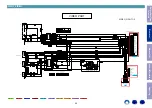
L105
3
C
B
05
Y
TY
H
221-201
2
DR
_T
X
C
K
DR
_T
X
C
K
B
DDR_1.8V
DGND
DR_TXBA2
DDR_1.8V
DR_TXDQ4
DDR_1.8V
DR_TXDQ6
DDR_1.8V
DR_TXDQ12
DDR_1.8V
DR_TXDQ14
DR_1_RFU1
DR_1_RFU2
DR_TXA9
DR_TXA11
DR_TXA5
DR_TXA6
DR_TXA1
DR_TXA2
DDR_1.8V
DR_TXBA1
DR_TXCASB
DR_TXWEB
DR_TXRASB
DDR_1_ODT
DGND
DDR_1.8V
DR_TXDQ3
DR_TXDQ2
DR_TXDQ5
DDR_1.8V
DDR_1.8V
DDR_1.8V
DR_TXDM0
DR_TXDQS0
DR_TXDQ7
DGND
DDR_1.8V
DR_TXDQ11
DR_TXDQ10
DR_TXDQ13
DDR_1.8V
DDR_1.8V
DDR_1.8V
DR_TXDM1
DR_TXDQS1
DR_TXDQ15
DR_TXA12
DR_TXA7
DR_TXA3
DR_TXA10
DR_TXBA0
DR_TXCKE
TX_DDRVREF
DGND
DR_TXDQ17
DGND
DGND
DR_TXDQ25
DGND
DR_2_RFU3
DR_TXA8
DR_TXA4
DR_TXA0
DR_TXCSB
DR_TXCKB
DR_TXCK
DR_TXDQ16
DR_TXDQSB2
DR_TXDQ24
DR_1_RFU3
DR_1_RFU2
DR_1_RFU1
TX_DDRVREF
DDR_1_ODT
R1717
10K
DDR_1.8V
DGND
DDR_1.8V
TO
ADV8003
TO
ADV8003
DR_TXDQSB3
DR_2_RFU3
DR_2_RFU2
DR_2_RFU1
TX_DDRVREF
DDR_2_ODT
R1718
10K
R
171
3
O
PE
N
100
N
-K
C
166
9
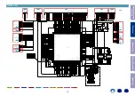
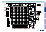
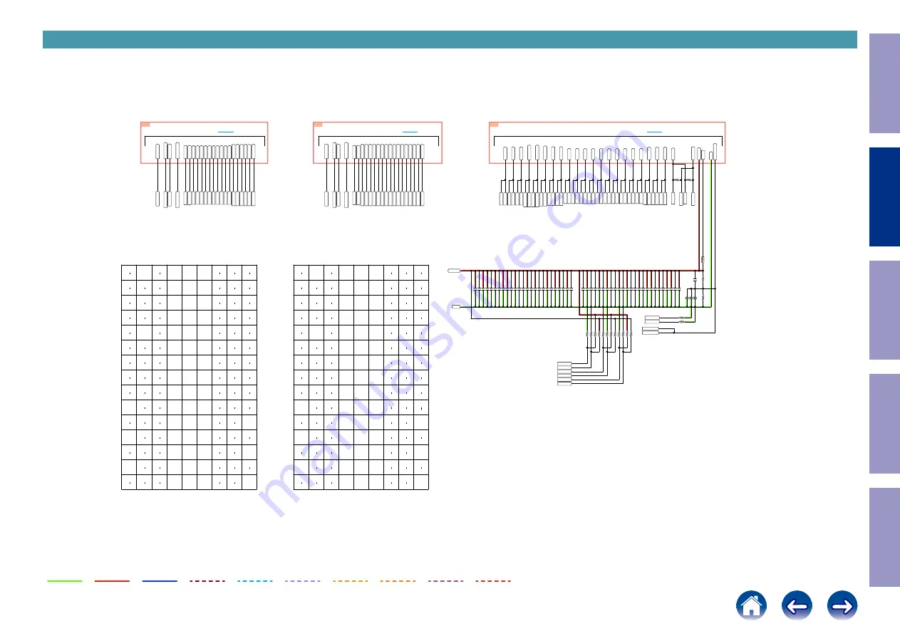
ADV8003 DDR
P2
K2
F2
B2
L2
J2
E2
A2
L3
J3
M2
H2
H1
F1
D2
D1
B1
P3
M3
K3
H3
F3
D3
B3
P8
P7
M8
M7
K8
K7
H8
H7
F8
F7
D8
D7
B8
B7
P9
M9
K9
H9
F9
D9
B9
R2
N2
R1
N1
L1
G2
C2
J1
G1
E1
C1
A1
R3
N3
G3
E3
C3
A3
L8
R8
N8
R7
N7
L7
J8
E8
G8
C8
J7
G7
E7
C7
A8
A7
J9
G9
E9
C9
A9
R
P
N
M
L
K
J
H
9
8
7
3
2
1
G
F
E
D
C
B
A
U1029
A3R12E40DBF-8E(512Mb)
P2
K2
F2
B2
L2
J2
E2
A2
L3
J3
M2
H2
H1
F1
D2
D1
B1
P3
M3
K3
H3
F3
D3
B3
P8
P7
M8
M7
K8
K7
H8
H7
F8
F7
D8
D7
B8
B7
P9
M9
K9
H9
F9
D9
B9
R2
N2
R1
N1
L1
G2
C2
J1
G1
E1
C1
A1
R3
N3
G3
E3
C3
A3
L8
R8
N8
R7
N7
L7
J8
E8
G8
C8
J7
G7
E7
C7
A8
A7
J9
G9
E9
C9
A9
R
P
N
M
L
K
J
H
9
8
7
3
2
1
G
F
E
D
C
B
A
U1028
A3R12E40DBF-8E(512Mb)
9D
0E
1E
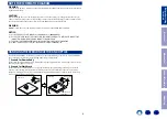
Before Servicing
This Unit
Electrical
Mechanical
Repair Information
Updating
17


