background image

22

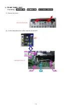
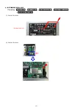
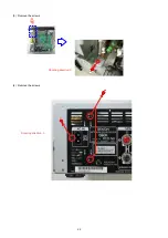
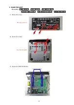
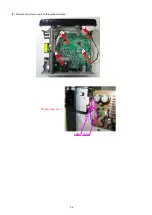
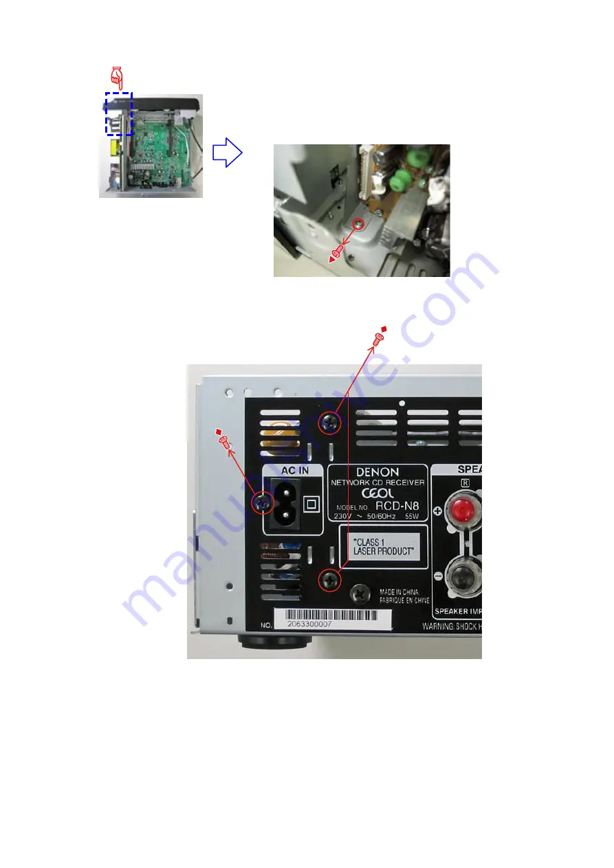
(3)  Remove the screws.

(4)  Remove the screws.

Shooting direction: C

Shooting direction: A

Summary of Contents for CEOL RCD-N8

Page 1: ...manual are slightly different from the actual set Please use this service manual with referring to the operating instructions without fail For purposes of improvement specifications and design are subject to change without notice The part list can be found in a separate file See the part list in Excel format Please refer to the MODIFICATION NOTICE ...

Page 2: ...de Factory Reset 26 2 Initialization mode User Reset 27 3 Version display 27 4 CD test mode 29 5 CD heat run mode 32 6 Product Mode 1 34 7 Product Mode 2 34 8 Protection history display mode 34 9 Update mode by disc 36 10 DPMS UP date mode 37 11 MAC Address rewrite mode 39 12 Access to development server mode 39 ABOUT REPLACE THE MICROPROCESSOR WITH A NEW ONE 40 VERSION UPGRADE PROCEDURE OF FIRMWA...

Page 3: ... same as before the jump Search for a Ref No phrase Ctrl Shift F You can use the search function in Acrobat Reader to search for a Ref No in schematic diagrams printed wiring board diagrams block diagrams and parts lists 1 Press Ctrl Shift F on the keyboard The Search window appears Ctrl Shift F 2 Enter the Ref No you want to search for in the Search window and then click the Search button A list ...

Page 4: ... The selected area is magnified Ctrl Space 0 When you want to move the area shown hold down Space and drag the mouse When you want to show a full page view press Ctrl 0 on the keyboard Properties Click this button and check that the printer is set to a suitable paper size Page to print Select the following checkbox More Options Current View Page Sizing Handling Select the following checkbox Size S...

Page 5: ...creen Example using Adobe Reader 9 On the Tools menu point to Select Zoom and then click Pan Zoom Window Magnify schematic printed wiring board diagrams 3 Loupe Tool function The Loupe Tool function lets you magnify a specific part of a diagram in a separate window Example using Adobe Reader X On the View menu point to Zoom and then click Loupe Tool The Loupe Tool window appears on the screen Exam...

Page 6: ...ortant safety parts that are indicated by the z mark on schematic diagrams and parts lists be sure to use the designated parts Be sure to mount parts and arrange the wires as they were originally placed For safety seasons some parts use tapes tubes or other insulating materials and some parts are mounted away from the surface of printed circuit boards Care is also taken with the positions of the w...

Page 7: ...RC Composition RS Metal oxide film RW winding RN Metal film RK Metal mixture P Pulse resistant type NL Low noise type NB Non burning type FR Fuse resistor F Lead wire forming 2B 1 8 W 2E 1 4 W 2H 1 2 W 3A 1 W 3D 2 W 3F 3 W 3H 5 W F 1 G 2 J 5 K 10 M 20 Ex RN Type 14K Shape and per formance 2E Power 182 Resist ance G Allowable error FR Others Resistance 1800ohm 1 8kohm 1 8 2 Indicates number of zero...

Page 8: ...perly grounded to remove any static electricity that may be charged on the body 2 Ground for Workbench Be sure to place a conductive sheet or copper plate with proper grounding 1 MΩ on the workbench or other surface where the semi conductors are to be placed Because the static electricity charge on clothing will not escape through the body grounding band be careful to avoid contacting semi conduct...

Page 9: ...ds Conforming to IEEE 802 11b Conforming to IEEE 802 11g Conforming to Wi Fi z Transfer rate DS SS 11 5 5 1 Mbps Automatic switching OFDM 54 48 36 24 18 12 9 6 Mbps Automatic switching Security SSID Network name WEP key network key 64 128 bits WPA PSK TKIP AES WPA2 PSK TKIP AES Used frequency range 2 412 MHz 2 472 MHz No of channels Conforming to IEEE 802 11b 13ch DS SS Of which 1 channel used Con...

Page 10: ...10 DIMENSION 299 0 112 0 108 0 35 0 35 0 210 0 280 0 2 0 301 0 218 0 45 0 36 0 30 0 4 0 ...

Page 11: ...E with the E2 963189100410D JP 963189100420D MAC Address was written 2 The firmware is updated by DPMS Refer to VERSION UPGRADE PROCEDURE OF FIRMWARE 2 How to update by DPMS page 41 for the details of the Version up 3 MAC Address Label pasted to Bottom is pasted to Mac Address Label GEN8341 MAC ADDRESS SUB ASSY of exchanged WLAN MODULE and it substitutes it CAUTION IN SERVICING ...

Page 12: ...ultaneously Factory Reset 3 Turn off the power using ON STANDBY button unplug the power cord 4 Plug the power cord into a power outlet while pressing VOLUMEd and f button simultaneously User Reset Service tools Measuring Disc CD TCD 784 CD R TCD R082W CD RW TCD W082W z Refer to MEASURING METHOD AND WAVEFORMS Note All user settings will be lost and this factory setting will be recovered when this i...

Page 13: ...nism prior to anchoring in the set should be protected against static electricity and dust The mechanism must be stored that damaging outside forces are not received When carrying the finished mechanism hold it by the chassis body For proper operation storage and operating environment should not contain corrosive gases For example H2S SO2 NO2 CI2 etc In addition storage environment should not have...

Page 14: ...s on the edges of top cover which could cause injury if fingers are moved across them Use gloves to protect your hands SIDE PANEL CD MECHA ASSY Refer to DISASSEMBLY 2 CD MECHA ASSY and EXPLODED VIEW CD MECHA ASSY Ref No of EXPLODED VIEW 10 MAIN PCB ASSY Refer to DISASSEMBLY 2 MAIN PCB ASSY and EXPLODED VIEW MAIN PCB ASSY Ref No of EXPLODED VIEW P2 FRONT PANEL ASSY Refer to DISASSEMBLY 3 FRONT PANE...

Page 15: ... Shooting direction A B C D Refer to the diagram below about the shooting direction of each photograph Photographs with no shooting direction indicated were taken from the top of the set The photograph is RCD N8 E2 model The viewpoint of each photograph Shooting direction View from the top Front side Shooting direction A Shooting direction B Shooting direction D Shooting direction C ...

Page 16: ...6 1 TOP COVER 1 Remove the screws 2 Remove the screws 3 Remove the connector wire Proceeding SIDE PANEL TOP COVER Shooting direction C Shooting direction D Shooting direction A CP303 Shooting direction A ...

Page 17: ...rcuit in Pick up of CD MECHANISM ASS Y then disconnect the connector wires and FFC cable Be sure to wear a grounding band 3 Remove the connector wire Proceeding SIDE PANEL TOP COVER CD MECHA ASSY FFC Shooting direction A Soldering place Shooting direction C ...

Page 18: ...T PANEL ASSY 1 Remove the screws 2 Cut the clamp bands remove the connector wire and FFC Proceeding SIDE PANEL TOP COVER FRONT PANEL ASSY View from the bottom CP301 CON2 CON1 CP104 Cut CN401 Shooting direction D ...

Page 19: ...19 3 Remove the screws Shooting direction C Shooting direction D Please refer to EXPLODED VIEW for the disassembly method of FRONT PANEL ASSY ...

Page 20: ...20 4 NETWORK PCB ASSY 1 Remove the screws 2 Remove the screws Proceeding SIDE PANEL TOP COVER CD MECHA ASSY FRONT PANEL ASSY NETWORK PCB ASSY Shooting direction A ...

Page 21: ...21 5 SMPS PCB ASSY 1 Remove the screws 2 Remove the screws Proceeding SIDE PANEL TOP COVER CD MECHA ASSY FRONT PANEL ASSY SMPC PCB ASSY View from the bottom CN221 CN222 Shooting direction C ...

Page 22: ...22 3 Remove the screws 4 Remove the screws Shooting direction C Shooting direction A ...

Page 23: ...Y 1 Remove the screws 2 Remove the screws 3 Remove the SUPPORT MECHA Proceeding SIDE PANEL TOP COVER CD MECHA ASSY FRONT PANEL ASSY NETWORK PCB ASSY MAIN PCB ASSY Shooting direction A View from the bottom SUPPORT MECHA ...

Page 24: ...24 4 Remove the screws remove the connector wires CN221 CN222 Shooting direction C ...

Page 25: ...OSE Servo adjustment Leaser current ON time 5 Heat Run mode ON STANDBY SOURCE Heat run 6 Product mode 1 VOLUME UP CURSOR RIGHT Factory use 7 Product mode 2 VOLUME UP CURSOR LEFT Factory use 8 Protection history mode CURSOR RIGHT VOLUME DOWN To view a history of only one of the most recent protection 9 Update mode by disc VOLUME DOWN CURSOR UP Development Factory use The details cannot be disclosed...

Page 26: ... display 2 seconds Power LED White lighting 2 seconds All off display 2 seconds Power LED Red Green lighting 2 seconds Factory Reset displayed for 5 seconds Initialization Items Default setting Default source Internet Radio TUNER band FM SDB OFF BASS 0 dB TREBLE 0 dB BALANCE CENTER DIMMER 100 VOLUME 5 TUNER Preset Favorite list Clear all Favorite list Clear all Clock 00 00 JP EU TIMER EVERYDAY ONC...

Page 27: ...otection not cleared Can erase the Recently Played list Startup display Initialized displayed for 5 seconds 3 Version display Menu items appear in the Add Version Otherwise normal operation To exit this mode unplug the power cord Startup display Version displayed for 5 seconds How to Display Version Press SOURCE and Cursor u Cursor i to select the Setup Press 1 3 ENTER button Internet Radio Music ...

Page 28: ...etup Press 1 3 ENTER button The version of the System u com Press Cursor i The version of the boot loader System u com Press Cursor i The version of the boot loader Network u com Press Cursor i The version of the image Network u com ...

Page 29: ...and set the disc Even if the disc is the tray must let OPEN CLOSE 4 2 Servo check Press 1 3 ENTER button Execute the following steps 1 3 ENTER button continuously for over 1 second to switch directly to SUB CODE readout in step t Press the SOURCE button to return to 0 CD TEST MODE q LD ON w FOCUS ON e CLV ON 1 3 ENTER button 1 3 ENTER button 1 3 ENTER button 1 3 ENTER button ...

Page 30: ...the error count 4 3 Pickup movement In the stop mode pickup moves in FWD outwards or REV inwards direction when Cursor p or Cursor o button pressed Pickup movement stops when button released Pickup moves while button is pressed When Cursor o button pressed move to stop operation after detection that inner switch has turned on 1 3 ENTER button Cursor p button Cursor o button Cursor p button Cursor ...

Page 31: ...FFSET uRFRP Caution If you have not completed the adjustment the value is not correct 4 5 All servo on and auto adjustment When VOLUME d button is pressed for over 1 second while the Unit is in the CD TEST MODE the laser turns on and the laser current is measured The laser drive current undergoes A D conversion for calculation The decimal point is omitted The current value is updated every 3 secon...

Page 32: ...on shipment from the factory and when the mechanism is replaced 5 CD heat run mode Heat run mode Startup display Heatrun Mode displayed for 5 seconds Press the Cursor u i button to switch the mode H R Normal H R Short H R Chacking After loading the disc press 1 3 ENTER button While heat run the operation of each button is not valid If an error occurs display the error and stop operation at that po...

Page 33: ... E1 00 Disc cannot be detected E1 01 Tracking offset adjustment not possible E1 02 Focus offset adjustment not possible E2 00 Focus servo dropped during playback E2 01 Focus servo dropped during searching E2 03 Focus servo dropped during TOC reading E2 05 Focus servo dropped during manual search E2 10 Subcode can no longer be read during playback E2 11 Subcode can no longer be read during searchin...

Page 34: ...o operation and Stop state USB iPod No Connection or Unsupported Disc or continue no operation and Stop state Network No Connection or Unsupported Disc or continue no operation and Stop state DIGITAL IN No Input unlock And continue no operation Portable In No Input no connection of terminal And continue no operation ANALOG IN Continue no operation To exit this mode unplug the power cord 8 Protecti...

Page 35: ...ion digital amplifier Protection history is reset When the Cursor u button is pressed for over 5 seconds while the protection history is displayed the count value is reset After the reset is complete the display No Protection Protection history is not cleared even when the set is reset User Reset ...

Page 36: ... Refer to VERSION UPGRADE PROCEDURE OF FIRMWARE 1 How to update by disc Upgrade by DPMS This mode describes a display only To exit this mode unplug the power cord Startup display Disc Update Mode displayed for 5 seconds The tray will open Insert disc The following states are displayed Display update file Updating display ...

Page 37: ...the update in an environment that has little network load 04 Firm Info response acquisition error recived Check the network connection Carry out the update in an environment that has little network load 05 Firm Info response acquisition TimeOut Check the network connection Carry out the update in an environment that has little network load 06 All Firm Info response acquisition error recived Check ...

Page 38: ... automatically 36 Login failure DPMSAccess Login incorrect infomation Carry out the update in an environment that has little network load 37 Login failure DPMSAccess Server busy infomation Carry out the update in an environment that has little network load 38 Login failure DPMSAccess connection failed infomation Check the network connection Carry out the update in an environment that has little ne...

Page 39: ...ection Carry out the update in an environment that has little network load AA After download request Login Failed Check the network connection Carry out the update in an environment that has little network load AB After download request Login Failed Check the network connection Carry out the update in an environment that has little network load AC After download request Login Failed Check the netw...

Page 40: ...iting procedure when you should be write in the software VERSION UPGRADE PROCEDURE OF FIRMWARE NOTE When you replace the RCD N8 WLAN MODULE 963189100420 you need software updates Refer to CAUTION IN SERVICING ABOUT REPLACE THE WLAN MODULE WITH A NEW ONE 1 How to update by DISC 1 1 Procedure of making CD R 1 Please download zipped file and unzip on your PC For JP RCDN8JP_xxxxxxxxxxxx xxxx zip 2 The...

Page 41: ...cessor and Version b While updating firmware any buttons of R C and Front panel are not worked Order of updating q System microprocessor approximately 5minits w Network microprocessor Boot Loader approximately 5minits Only If you need to update e Network microprocessor image approximately 30minits 7 After 35 minutes unit will be updated completely and open the tray automatically 8 Remove CD R and ...

Page 42: ...1 Erase failure 32 Write failure 33 Verify incorrect 34 Communication error B2 DM8x0 firmware rewrite error information received 1 4 Notice of updating firmware 1 When unit is updating firmware on item 1 2 Procedure of updating 6 do not turn off the power or pull out AC cord from AC wall socket 2 If power supply stop to supply microprocessor unit will be broken q When AC cord is pulled while updat...

Page 43: ...f the latest firmware version is on the web proceed to 4 If the latest firmware is already installed press the SOURCE button to close the Update menu 4 Press 1 3 ENTER button Select YES then press 1 3 ENTER button 5 Firmware Update will be started Cautions on Firmware Update In order to use these functions you must have the correct system requirements and settings for a broadband Internet connecti...

Page 44: ...upply Voltages for System µ com MAIN B D 5V_SMPS1 CN408 9pin 3 3V_CPU IC402 4pin Check Drive Signals for OLED DISPLAY B D CN661 D0 D7 EL_RD EL_RW EL_DC EL_CS EL_RST END Check Soldering IC402 on MAIN B D CN408 9pin SMPS B D Check Soldering IC404 IC403 Check Soldering RES401 on MAIN B D Check Soldering IC406 on MAIN B D CN401 on MAIN B D CN661 on DISPLAY B D CP661 on DISPLAY B D Check Soldering IC40...

Page 45: ... H level O K Check Oscillation waveform MAIN B D IC103 40pin TXO 24 576MHz OK Check Oscillation waveform MAIN B D IC108 19pin XTL_O 13 5MHz OK IC108 63pin MCLK MCLK OK Check Soldering IC102 IN 12V_A OUT 5V_A IC401 IN 5V_SMPS1 OUT 3V3_D1 POWER B D Check Soldering R238 R239 R240 3V3_5508 Check Soldering IC403 68pin DIR_RESET on MAIN B D Check Soldering IC403 77pin 5508_RESET on MAIN B D Check Solder...

Page 46: ... OK OK 2 2 CD PLAY BACK Check control signal for DIR MAIN B D IC103 23 24 25 26pin DIR_D0 DIR_DI DIR_CL DIR_CE Check Soldering IC403 86 87 88 89pin DIR_D0 DIR_DI DIR_CL DIR_CE NG OK Check control signal for PWM CONTROLLER MAIN B D IC108 24 25pin 5508_SDA 5508_SCL IC108 13 14pin PDN MUTE H level O K END Check Soldering IC403 82 83pin 5508_SDA 5508_SCL on MAIN B D IC108 13 14pin PDN MUTE on MAIN B D...

Page 47: ... 44 45 46 47pin Check PWM Audio Data output for PWM CONTROLLER MAIN B D IC118 4 6 14 16 pin Check Audio Data output from AMP to SPEAKER MAIN B D IC118 22 25 30 33 pin JACK105 OK OK OK Check Soldering IC108 26 27 28pin on MAIN B D Check Soldering IC108 on MAIN B D Check Soldering IC118 on MAIN B D Check Soldering IC118 on MAIN B D JACK105 on MAIN B D NG NG NG NG END ...

Page 48: ... H Check the Output form Analog selector IC701 15 2pin TU_L TU_R 5 7pin AIN_CNT1 2 L L Check the DIR input IC103 47 48 AIN_L AIN_R Check the input of DIR IC103 47 48 AIN_L AIN R OK OK OK OK OK OK OK Check Soldering IC102 IN 12V_A OUT 5V_A CN408 3pin 12V_A Check Soldering JK632 on FRONT B D CP631 on FRONT B D Check Soldering C761 C768 Check Soldering IC403 69 70pin AIN_CNT1 2 Check Soldering IC403 ...

Page 49: ... 1 H L AUX 2 Check Digital Audio Data from OPTICAL Input IC MAIN B D IC103 28pin OPT_IN Check the input of DIR 2 IC103 47 48 AIN_L AIN_R OK OK OK OK OK Check Soldering JACK102 on MAIN B D Check Soldering JACK101 3pin 3V3_D1 IC401 IN 5V_SMPS1 OUT 3V3_D1 CN408 9pin 5V_SMPS1 SMPS B D Check Soldering 1 IC403 69 70pin AIN_CNT1 2 Check Soldering IC103 OPT_IN on MAIN B D Check Soldering 3 C125 C124 on MA...

Page 50: ...870_SPDIF MAIN B D CP201 24pin CX870_SPDIF OK OK OK OK OK OK Check Soldering Network B D CP302 24 25pin 5V_NET CP302 28 29pin 5V_VBUS MAIN B D CP201 5 6pin 5V_NET CP201 1 2pin 5V_VBUS CN408 10pin 5V_NET CN408 11 12pin 5V_SMPS2 SMPS B D Check Soldering CP301 5 6pin 5V on Network B D CN641 1 2pin 5V on DISPLAY B D JACK641 on DISPLAY B D Check Soldering CP303 1pin 5V on ETHERNET B D CN303 1pin 5V on ...

Page 51: ...R902 R901 C901 CN408 C913 C191 IC903 IP4001CR IC118 TAS5142DKD C942 AZ1117H 1 5 IC901 C224 R229 C227 R231 R233 C219 C222 L109 JACK104 JACK105 L108 IC902 TC94A92FG 301 R472 R473 R507 R477 Q121 JACK102 AUX R5F56108VNFP IC403 3300 50 C171 TDI TXD RESET WPS f KEY1 KEY3 D1 KEY2 b D5 D7 EL_CS e JP E3 E2 D2 D0 D4 R434 OPEN 1K 1K 20 1 10 c 15 5 45 40 140 130 25 PCM9211 35 30 40 15 120 5 90 80 100 110 k AZ...

Page 52: ...D Q2 CN26 1 LOAD Q3 R407 LRCK Q4 R408 SCLK Q5 R409 SDATA C946 C941 C944 C969 C908 C981 C948 R914 C968 C905 C962 C916 L902 C938 C939 R725 C975 C284 C903 R721 R915 C929 C943 C935 L906 D902 D104 C917 R728 C976 R727 R726 R923 R921 D282 R922 R722 R723 Q901 C970 C928 C936 C947 C950 L908 C915 C286 D284 D286 R916 C902 C253 C251 C252 LOAD LOAD OP_SW CL_SW GND_DRV SP SLED SLED SP INSW GND_DRV Q0 Q1 Q2 o C q...

Page 53: ...DW082W PLAY 1 2 CD R TCDR082W PLAY CD TCD784 DETECTION 2 3 CD RW TCDW082W DETECTION 2 2 CD R TCDR082W DETECTION wRFO eFEI rFOO tTEI yTRO uFMO iDMO wRFO eFEI rFOO tTEI yTRO uFMO iDMO CD TCD784 READ 1V div 500mV div 1V div 1V div 1V div 500mV div 1V div 1V div 500mV div 1V div 1V div 1V div 500mV div 1V div 1V div 500mV div 3 3 CD RW TCDW082W READ 3 2 CD R TCDR082W READ CD TCD784 FOCUS ADJUSTMENT 4 ...

Page 54: ...54 5 CD Playback 6 LOADER OPEN CLOSE Q3LRCK Q4SCLK Q5SDATA STANDARD GND STANDARD GND WF12 9 oOPSW Q0FCLSW Q2LOAD Q1LOAD OPEN CLOSE ...

Page 55: ...or Up Cursor Down Cursor Right Cursor Left Enter Vol Up Vol Down RJ 45 IC108 PWM PROCESSOR TAS5508 IC118 D Amp TAS5142 SPK OUT L SPK OUT R IC103 DIR PCM9211 MUTE I2S A D OLED S020 MXS4035A USB2 0 Switcher P_DOWN 50 60 Puls SUB_POWER_CONT 5V_SMPS1 5V_SMPS 5V_NET 12V_A 12V_A 12V_D 29V_DAMP 18V_OLED Power LED IR Ethernet MUTE Filter Filter FRONT B D MAIN B D SWITCHED MODE POWER SUPPLY Differential Di...

Page 56: ..._D2 KIA78R33F 3 3V_D2 D3 IC902 TC94A92FG 301 IC901 1 5V_D2 D3 IC902 TC94A92FG 301 AZ1117H 1 5TRE1 Q406 5V_VBUS LED_W 5V_VBUS LD601 KRA102S IC301 5V_VBUS 5V_VBUS IC310 NCP380 5V_VBUS 5V_VBUS NCP380 Q303 5V_NETN USB_VBUSN IC306 KRA102S NET_ 3VN3 NET_ 3 3V AP3503E NET_ 3 3V NET_ 3 3V IC125 MFI337S3959 NET_ 3 3V IC303 IC304 TC7USB221FT IC307 NET_ 1VN9 NET_ 1 9V AP3503E IC308 NET_ 1VN2 NET_ 1 2V AP3503...

Page 57: ...GND_D 15 NWAIT 16 RXD1 17 NCS2 18 TXD1 19 NRESET_MOD 20 GND_D 21 3V3RTC 22 AV2CTRL1 23 GND_D 24 AV2CTRL0 25 SPI_DIN 26 AV2CLK 27 SPI_DOUT 28 AV2DATA2 33 GPIO17 34 AV4DATA0 35 GND_D 36 GND_D 37 GPIO11 38 USB_DN 39 AV3CTRL1 40 USB_DP 41 AV3CTRL0 42 USBVBUSDRV 43 GND_D 44 USB_VBUS 45 PDOUT1 46 GND_D 47 PDOUT0 48 GPIO09 49 VCO0 50 GPIO08 51 GND_D 52 GND_D 53 ETH_LED_SPEED 54 ETH_LED_ACT 55 MIITXCLK 56...

Page 58: ...ND_D KEY1 H P_L GND_A GND_A H P_R AUX_R GND_A VLSS D7 CLS D5 D4 D3 D2 BS0 BS1 CL NC VCI VSL VLSS AUX IN DOWN ENTER GND_D RED D2 GND_D D7 EL_E RD 16V_OLED VCOMH D1_SDIN E RD R W WR D C GND_D VDDIO I REF 16V_OLED LEFT UP GND_D SOURCE POWER RED GREEN LED AUX_L 16V_OLED 16V_OLED 3 3_CPU EL_R W WR EL_RESET D6 CS VDD H P VOL_DN V0L_UP NETWORK STBY OP CL LED_GREEN GND_D D0_SCLK RES RIGHT WHITE LED LED SE...

Page 59: ...R332 L305 IC307 AP3503E IC305 R344 C304 C301 CP303 BKT302 SW401 BKT301 JACK301 U100 CP302 VBUS VBUS GND_D DATA DAAT GND_D VBUS GND_D DATA DATA GND_D ACC_MODE WPN NC RXD GND NC NC 3 3V TXD BURRING GND_D AP3503E AP3503E AP3503E NCP380 5V_VBUS 5V_VBUS NCP380 GND_D GND_D MFI337S3959 USB_OE B1 B2 IPOD_DET E_P_CONT E_SPICS E_TXDMIEO E_SPIMOEI E_SPIMIEO E_SPICLK E_REQ VBUS_FLUG2 GND_D ACC_MODE CX870_SPDI...

Page 60: ...C965 C967 R934 R930 R928 R937 R936 R935 R942 C966 R943 C973 C971 R926 R944 R948 R902 R901 C901 CN408 C913 C191 IC903 IP4001CR IC118 TAS5142DKD C942 AZ1117H 1 5 IC901 C224 R229 C227 R231 R233 C219 C222 L109 JACK104 JACK105 L108 IC902 TC94A92FG 301 R472 R473 R507 R477 Q121 JACK102 AUX R5F56108VNFP IC403 3300 50 C171 TDI TXD RESET WPS f KEY1 KEY3 D1 KEY2 b D5 D7 EL_CS e JP E3 E2 D2 D0 D4 R434 OPEN 1K...

Page 61: ... GND_A R119 680 C114 12P J 15P J C115 TO AMP BLOCK C122 10 16 MVG C117 4N7 C125 22 16 MVG 1000 16 C417 R113 OPEN OPEN C126 10P J C127 10P J 470 16 C420 1SS355 D405 OPEN R127 EMULATOR CP403 MP OPEN 2 4 6 8 10 5 3 1 7 9 11 OPEN 11P FFC CP405 OPEN R415 3V3_CPU KRC102S Q403 3V3_CPU 3V3_CPU 100N K C436 1N K C433 1N K C431 C432 10N K 33 R436 R527 33 C461 100N K 10N K C460 R442 4K7 1N K C442 10N K C441 O...

Page 62: ... 10K R382 100 R385 OPEN 100N K C377 WPSN WPS RD N R348 10K C376 100N K NET_ 3VN3 NET_ 1VN9 C360 GND GND NCS2 GND GND GND C379 100N K L311 0 R360 0 R362 75 0 R376 L314 BD102 C363 22 16 100N K C355 R352 0 USB DATAN E_RXDMOEIN BKT301 C367 OPEN C368 OPEN GND_D R366 OPEN FGN6 R353 100 TXD1 L701 BLM21PG221 10N K C312 R378 100K C391 100P J OPEN R317 R312 47K 27K R306 47K R305 5V_NET_DN OPEN R323 Q301 OPE...

Page 63: ...PEN GND_DRV 7V5_D1 3V3_D1 C932 100 10 SE 220 R927 C951 100N K C933 100 10 SE 15K R934 DRVMUTE 10K R943 C969 100N K 100 R909 0 R911 0 R913 10K R949 100N K C976 10K R945 10K R947 R910 47K CD_SPDIF GND_DA 47 R914 TO CD MECHA 1 3 5 7 29 9 11 13 28 26 24 22 30 20 18 16 2 4 6 8 10 14 12 27 25 23 21 19 15 17 IN1 N C FIN FWD REV DO1 PGND2 DO4 IN4A VCC2 FIN CTL DO2 DO3 PGND1 DO5 DO5 IN1A REO SGND IN2 DO1 D...

Page 64: ...110 KRC102S 3V3_D1 3 3V_D1 GND_AD KDS4148U D110 D112 KDS4148U 12V_D 100N K C231 SP_PROTECT GND_AD 100N K C233 12V_5142 R289 0 3216 R297 0 2012 R282 0 2012 R391 0 2012 10K R173 12V_5142 12V_5142 C220 47 25 LA RA C237 220 25 8 11 5 C156 100N K R175 10 R255 0 L105 BD221JT R226 22K R215 39K C213 100P J 47 50 MVG C250 C224 10N K 47 50 MVG C248 GND_AD 2 1 4 3 INDUCTOR_10UH L109 R232 10K R233 4K7 2 1 4 3...

Page 65: ...270 R610 LD602 RIGHT DOWN R616 150 S605 S606 ENTER R613 150 R608 150 S601 S602 VOL_DN S608 VOL_UP R615 270 R612 270 S604 TO CPU R653 0 C660 OPEN L641 AXIAL BEAD C682 1N K C685 OPEN C650 OPEN C651 OPEN C652 OPEN CLAMP TO NETWORK C655 100P J OPEN C606 OPEN C609 47K R651 C656 100P J C659 100N K 1000N Z C663 EL_RW EL_CS C680 47P J 16V_OLED 10 35 5 5 C675 L662 BLM11A121 10N K C671 LED_GREEN Q601 KRC111...

Page 66: ... 104 2012 C252 334 2012 R255 1 5KF 2012 R254 15KF 2012 R253 1 8KF 2012 R871 100K 1W C872 103K 630V D871 UF4007 B871 3550 R873 0 3216 R874 10 3216 D872 BAV21W D874 BAV21W D442 HS1M C443 25V 220uF 105 L442 4 7uH DR2 C444 25V 100uF 105 C445 104 2012 C441 10V 2200uF 105 C442 10V 470uF 105 L441 5 5uH BAR 1 2 PC871 A PC17K 1 3 4 PC871 B PC17K 1 R452 470 2012 R451 470 2012 R453 5 1KF 2012 R455 1K 2012 C4...

Page 67: ... S2 3 S1 8 S1 6 S2 3 S1 7 S1 3 S3 4 41 S1 6 S4 3 S1 2 S5 12 16 43 S1 4 for WH S1 2 S6 4 for BK S1 3 for WH model S6 3 for BK model S1 4 for WH model S6 4 for BK model S2 8 S1 8 44 45 46 Parts marked with this symbol have critical characteristics Use ONLY replacement parts recommended by the manufacturer WARNING 印の部分は安全を維持するために重要 な部品です 従って交換時は必ず指定の 部品を使用してください ...

Page 68: ...LODED VIEW OF CD MECHANISM UNIT Parts marked with this symbol have critical characteristics Use ONLY replacement parts recommended by the manufacturer WARNING 印の部分は安全を維持するために重要 な部品です 従って交換時は必ず指定の 部品を使用してください ...

Page 69: ...which nsp is indicated on this table cannot be supplied When repairing the P W B ASS Y check the board parts table and order replacement parts zThe parts listed below are for maintenance only might differ from the parts used in the unit in appearances or dimensions zPart indicated with the mark is not illustrated in the exploded view Personal notes ...

Page 70: ...s indicated by nsp on this table cannot be supplied zParts indicated by the mark are not illustrated in the exploded view zThe parts listed below are only for maintenance Therefore they might differ from the parts used in the unit in appearances or dimensions Personal notes ...

Page 71: ...NG STYLE A 22 25 PE SHEET PACKING 9 3 22 ZIPPER TYPE 13 17 6 3 5 A 11 1 6 16 5 R R L L 7 25mm 20mm 25mm 15 BATT ERY DRY BATT ERY DRY 9 26 29 TOP NON SILK AR EA TOP NON SILK AR EA 24 8 10 18 2 14 9 4 28 27 Delete Carton position change Position change ...

Page 72: ... Please refer to the last chapter zParts for which nsp is indicated on this table cannot be supplied zThe parts listed below are for maintenance only might differ from the parts used in the unit in appearances or dimensions Personal notes ...

Page 73: ...TORS Only major semiconductors are shown general semiconductors etc are omitted to list The semiconductor which described a detailed drawing in a schematic diagram are omitted to list 1 IC s R5F56108VNFP MAIN IC403 ...

Page 74: ...I NMI PU I I I I Basic Functions of Microcomputer 25 P34 EL RESET PD O O L O L O L Reset for OLED L Reset 26 P33 EL E RD O O L O L O L EL Readout 27 P32 EL D C O O L O L O L Switching Data Commando H Data L Command 28 P31 EL R W WR O O L O L O L EL Writing 29 P30 EL CS O O L O L O L EL Chip Select L I F communication 30 P27 D7 O O L O L O L Data Bus for OLED 31 P26 D6 O O L O L O L Data Bus for OL...

Page 75: ...IN_CNT1 O O L O L O L Input Switching Control for Analog IN 1 71 PC5 OPEN O O L O L O L OPEN 72 PC4 TEMP_DET O O L O L O L OPEN 73 PC3 H P_MUTE PD O O L O L O L H P MUTE L MUTE H PLAY 74 VCC VCC 3 3V_CPU 75 PC2 AMUTE PD O O L O L O L SW MUTE 76 VSS VSS GND 77 PC1 5508_RESET PU O O L O L O L TAS5508 System Reset Input 11 pin 78 PC0 H P_ON PU O O L O L O L TAS5508 Headphone In Out Selector 12 pin 79...

Page 76: ...ault SBSY from CD DSP TC94A92FG 118 P60 DRVMUTE PU_OPEN O O L O L O L CD Driver Mute H Mute Off L Mute On 119 PD3 CD_OPEN O O L O L O L Open CD Tray 120 PD2 CD_CLOSE O O L O L O L Close CD Tray 121 PD1 VBUS_FLUG1 PU I I I I Check VBUS Voltage 1 Front USB L Error 122 PD0 VBUS_FLUG2 PU I I I I Check VBUS Voltage 2 iPod Dock L Error 123 P97 LD_CHK AD I I I O L Check CD Laser Diode Current 124 P96 VBU...

Page 77: ...MoN1 BUS2 64 37 Pio12 CDMoN0 FGiN BUS3 65 36 Pio11 BUCK 66 35 Pio10 CCE 67 34 Pio9 MS 68 33 Pio8 RST 69 32 VDD1 3 TEST 70 31 DMo VDD1 1 71 30 FMoS VSS 1 72 29 FMo SRAMSTB 73 28 VSS 3 VDDM1 74 27 TRo PDo 75 26 Foo TMAX 76 25 AVDD3 LPFN 77 24 TEi LPFo 78 23 RFRP PVREF 79 22 RFZi VCoF 80 21 FSMoNiT 1 2 3 4 5 6 7 8 9 10 11 12 13 14 15 16 17 18 19 20 VCoi RVDD3 SLCo RFi RFRPi RFEQo DCoFC AGCi RFo RVSS3...

Page 78: ...h C Pointer register Y Pointer register A3 X Pointer register Address Calc 2sets YRAM 4kw 24bit X Bus Y Bus 40bit XRAM 4kw 24bit ERAM 4kw 24bit CROM 4kw 11 44kw 24bit PRAM 1024w 40bit PROM 4kw 9 36kw 40bit General I O I F SRAM I F SRAM 512kbit 4kw 128bit MCU I F Pio0 7 Intrupt Cont IRQ Program Control Instruction Decoder round limit round limit TEi VREF 4KB SRAM Control Servo AVSS3 AVDD3 IP ATT VD...

Page 79: ...5uF 8 AGCi I 3AI F RF signal AGC amplifier input pin I 9 RFo O 3AI F RF signal generation amplifier output pin O 10 RVSS3 Grounding pin for 3 3 RF amplifier core and PLL circuit 11 FNI2 I 3AI F Main beam signal input pin To be connected to PIN diode C I 12 FNI1 I 3AI F Main beam signal input pin To be connected to PIN diode A I 13 FPI2 I 3AI F Main beam signal input pin To be connected to PIN diod...

Page 80: ... pin O Bulit in output R 3 3 kΩ 32 VDD1 3 I O 3I F Power supply pin for 1 5V Decoder DSP CD circuit 33 Pio8 I O 3I F Port 8 General Input Output Port I CMOS Port Schmitt input Refer to 1 2 Pin Assinment Table 34 Pio9 I O 3I F Port 9 General Input Output Port I CMOS Port Schmitt input Refer to 1 2 Pin Assinment Table 35 Pio10 I O 3I F Port 10 General Input Output Port I CMOS Port Schmitt input Refe...

Page 81: ...it 52 VSS 2 Grounding pin for 1 5V digital circuit 53 Pio0 I O 3I F Port 0 General Input Output Port I CMOS Port Schmitt input Refer to 1 2 Pin Assinment Table 54 Pio1 I O 3I F Port 1 General Input Output Port I CMOS Port Schmitt input Refer to 1 2 Pin Assinment Table 55 Pio2 I O 3I F Port 2 General Input Output Port I CMOS Port Schmitt input Refer to 1 2 Pin Assinment Table 56 Pio3 I O 3I F Port ...

Page 82: ... MS I 3I F Microprocessor I F mode selection pin H Parallel I F L Serial I F I Refer to 1 2 Pin Assinment Table 69 RST I 3I F Reset Input pin I Schmitt input 70 Test I 3I F Test pin L fixed I Connect to GND for normal operation 71 VDD1 1 Power Supply pin for 1 5V Digital circuit 72 VSS 1 Grounding pin for 1 5V Digital circuit 73 SRAMSTB I 3I F 1Mbit SRAM stand by pin SRAMSTB L I 74 VDDM1 Power Sup...

Page 83: ... NPN TR Built in mute circuit Built in Tray motor speed control circuit Wide operating supply voltage range 6 5V 13 2V Device Package Operating Temp IP4001 28SSOPH 375 35OC 85OC IP4001TF 28SSOPH 375 35OC 85OC BLOCK DIAGRAM ORDER INFORMATION FEATURES 8 9 10 11 12 13 14 2 3 4 5 6 7 1 21 20 19 18 17 16 15 27 26 25 24 23 22 28 DO1 DO1 IN1 IN1A N C REO MUTE SGND FWD IN2 DO2 DO2 PGND1 REV DO5 DO5 DO3 DO...

Page 84: ...84 PCM9211 MAIN IC103 ...

Page 85: ...85 PCM9211 Block Diagram ...

Page 86: ...86 PCM9211 Pin Discriptions ...

Page 87: ...87 NJM2755 MAIN IC701 NJM2755 Block Diagram ...

Page 88: ...C 24 30 P Power ground for half bridge C GND_D 23 29 P Power ground for half bridge D GVDD_A 36 44 P Gate drive voltage supply requires 0 1 µF capacitor to AGND GVDD_B 1 1 P Gate drive voltage supply requires 0 1 µF capacitor to AGND GVDD_C 18 22 P Gate drive voltage supply requires 0 1 µF capacitor to AGND GVDD_D 19 23 P Gate drive voltage supply requires 0 1 µF capacitor to AGND M1 13 15 I Mode ...

Page 89: ...and I O Logic PWM_C OUT_C GND_C PVDD_C BST_C Timing Gate Drive Ctrl PWM Rcv GVDD_C PWM_B OUT_B GND_B PVDD_B BST_B Timing Gate Drive Ctrl PWM Rcv GVDD_B PWM_A OUT_A GND_A PVDD_A BST_A Timing Gate Drive Ctrl PWM Rcv GVDD_A Ctrl BTL PBTL Configuration Pulldown Resistor BTL PBTL Configuration Pulldown Resistor BTL PBTL Configuration Pulldown Resistor BTL PBTL Configuration Pulldown Resistor Internal P...

Page 90: ...Pullup Headphone in out selector When a logic low is applied the headphone is selected speakers are off When a logic high is applied speakers are selected headphone is off LRCLK 26 DI 5 V Serial audio data left right clock sampling rate clock MCLK 63 DI 5 V Pulldown MCLK is a 3 3 V master clock input The input frequency of this clock can range from 4 MHz to 50 MHz MUTE 14 DI 5 V Pullup Soft mute o...

Page 91: ...ternal devices VR_DIG 33 P Voltage reference for 1 8 V digital core supply A pinout of the internally regulated 1 8 V power used by digital core logic A 4 7 µF low ESR capacitor 3 should be connected between this terminal and DVSS This terminal must not be used to power external devices VR_DPLL 17 P Voltage reference for 1 8 V digital PLL supply A pinout of the internally regulated 1 8 V power use...

Page 92: ... 7 Biquads DC Block De Emph SRC NS PWM 0 Det 7 Biquads DRC Loud Comp Soft Tone DC Block De Emph SRC NS PWM 8 2 Crossbar Mixer 0 Det 7 Biquads DRC Loud Comp Soft Tone DC Block De Emph SRC NS PWM 0 Det 7 Biquads DRC Loud Comp Soft Tone DC Block De Emph SRC NS PWM 0 Det 7 Biquads DRC Loud Comp Soft Tone DC Block De Emph SRC NS PWM 0 Det 7 Biquads DRC Loud Comp Soft Tone DC Block De Emph SRC NS PWM 0 ...

Page 93: ...93 L6565 SMPS IC821 L6565 Block Diagram ...

Page 94: ...94 ICE3BR1765J SMPS IC871 ICE3BR1765J Block Diagram ...

Page 95: ...95 2 DISPLAY S020 MXS4035A 3 DISPLAY CP661 ...

Page 96: ... refer to the last chapter zParts indicated by nsp on this table cannot be supplied zThe parts listed below are only for maintenance Therefore they might differ from the parts used in the unit in appearances or dimensions Personal notes ...

Page 97: ...160S 1 C658 nsp C CERAMIC CHIP HIK X7R0 01UF K 50V 1608REEL D011103777160S 1 C659 nsp C CERAMIC CHIP HIK X7R 0 1UF K 25V 1608REEL D011104774161S 1 C661 00D9630333300 C ELECT GE 85C 47UF M 16V 6 3 5 5RE SRE SY D040470083070S 1 C662 nsp C CERAMIC CHIP HIK X7R 0 1UF K 25V 1608REEL D011104774161S 1 C663 nsp C CERAMIC CHIP HIK Y5V1UF Z 50V 1608REEL D011105597160S 1 C664 nsp C CERAMIC CHIP HIK X7R 4 7UF...

Page 98: ...23 REEL J5200107S0050S 1 Q107 00D9630121606 SEMI CHIP TR NPN 2SC KRC107S NH SOT 23 REEL J522107S00210S 1 Q108 90M BA001600R SEMI CHIP TR PNP 2SA KRA107S PH SOT 23 REEL J5200107S0050S 1 Q110 111 00D2690192902 SEMI CHIP TR NPN 2SC KRC102S NB 0 2W SOT 23 REEL J522010200210S 1 Q112 113 90M BA001600R SEMI CHIP TR PNP 2SA KRA107S PH SOT 23 REEL J5200107S0050S 1 Q114 115 00D2690192902 SEMI CHIP TR NPN 2S...

Page 99: ...0002736M160S 1 R307 nsp R CHIP THICK 75K J 1 16W 1608REEL C20007536M160S 1 R309 nsp R CHIP THICK 120K J 1 16W 1608REEL C20001246M160S 1 R311 nsp R CHIP THICK 75K J 1 16W 1608REEL C20007536M160S 1 R312 nsp R CHIP THICK 47K J 1 16W 1608REEL C20004736M160S 1 R314 nsp R CHIP THICK 27K J 1 16W 1608REEL C20002736M160S 1 R315 nsp R CHIP THICK 120K J 1 16W 1608REEL C20001246M160S 1 R319 322 nsp R CHIP THI...

Page 100: ... 707 nsp R CHIP THICK 510K J 1 16W 1608REEL C20005146M160S 1 R708 709 nsp R CHIP THICK 0 J 1 16W 1608REEL C20000006M160S 1 R717 718 nsp R CHIP THICK 0 J 1 16W 1608REEL C20000006M160S 1 R731 734 nsp R CHIP THICK 0 J 1 16W 1608REEL C20000006M160S 1 R751 752 nsp R CHIP THICK 16K J 1 16W 1608REEL C20001636M160S 1 R753 754 nsp R CHIP THICK 15K J 1 16W 1608REEL C20001536M160S 1 R755 nsp R CHIP THICK 16K...

Page 101: ... 1 C209 00D2544573981 C ELECT GE 85C 10UF M 50V 5 11 5RE SMS SY D040100087070S 1 C210 nsp C CERAMIC CHIP T C COG100PF J 50V 1608REEL D010101167160S 1 C211 212 nsp C CERAMIC CHIP T C COG270PF J 50V 1608REEL D010271167160S 1 C213 214 nsp C CERAMIC CHIP T C COG100PF J 50V 1608REEL D010101167160S 1 C215 00D2544573981 C ELECT GE 85C 10UF M 50V 5 11 5RE SMS SY D040100087070S 1 C216 nsp C CERAMIC CHIP T ...

Page 102: ... K 50V 1608REEL D011104577160S 1 C414 nsp C CERAMIC CHIP HIK X7R0 01UF K 50V 1608REEL D011103777160S 1 C415 nsp C CERAMIC CHIP T C X7R 1000PF K 50V 1608REEL D010102777160S 1 C417 00D9609009940 C ELECT GE 85C 1000UF M 16V 10 16 L BLK SY D040102083030S 1 C418 419 nsp C CERAMIC CHIP HIK Y5V0 1UF Z 50V 1608REEL D011104597160S 1 C420 963134001860S C ELECT GE 85C 470UF M 16V 8 11 5 5RE SHL SY D040471083...

Page 103: ...608REEL D011103777160S 1 C959 00D2544302974 C ELECT GE 85C 100UF M 10V 6 3 5 5RE SY Pb Free SY D040101082130S 1 C960 nsp C CERAMIC CHIP HIK X7R2200PF K 50V 1608REEL D011222777160S 1 C962 963 nsp C CERAMIC CHIP HIK X7R0 1UF K 50V 1608REEL D011104577160S 1 C965 nsp C CERAMIC CHIP HIK X7R0 015UF K 50V 1608REEL D011153777160S 1 C966 nsp C CERAMIC CHIP HIK X7R0 1UF K 50V 1608REEL D011104577160S 1 C967 ...

Page 104: ...0 8t SCREW 4010210196100S 1 BKT301 302 nsp BRACKET AVR133 HARMAN BURRING HOLE SPTE 0 8t SCREW 4010210196100S 1 963189100410D CX870 3B D60 JUKEBOX NETWORK 2ANT 64MSDRAM NEW F W E2 RCDN8 8 9528E 12 1 963189100420D CX870 3B D60 JUKEBOX NETWORK 2ANT 64MSDRAM NEW F W JP RCDN8 8 9528E 12 1 963189100500S CX870 3B D60 JUKEBOX NETWORK 2ANT 64MSDRAM NEW F W E1C RCDN8 8 9525E 12 1 Ver 3 nsp HEAT SINK DRAF109...

Page 105: ...3020S 2 27 nsp BUSHING TERMINAL BLACK E2 E1C 2410040353010S 2 28 nsp PLATE TERMINAL 4470212666000S 1 29 nsp CHASSIS BOTTOM E2 3207214436000S 1 29 nsp CHASSIS BOTTOM JP 3207214436100S 1 29 nsp CHASSIS BOTTOM E1C 3207214436010S 1 Ver 3 30 nsp COVER SCREW 4310215316000S 1 31 nsp BRACKET SMPS 4010214936100S 1 32 963404100480S PANEL SIDE R WHITE 3060215751100S 1 Ver 3 32 963404100490S PANEL SIDE R BLAC...

Page 106: ...W 2S 3 8 ZNW BH BLACK B020030081B10S 46 S2 nsp SCREW 2S 3 8 BK FH B020030083F10S 14 S3 nsp SCREW 2S 3 10 ZNW BH B020030101B10S 8 S4 nsp SCREW 2S 2 6 8 BK BH B020026083B10S 3 S5 nsp SCREW 2S 3 10 DOT BK B020030103B11S 12 S6 nsp SCREW 2S 3 8 BK BH BLACK B020030083B10S 11 10 ...

Page 107: ...101420S CUSHION TOP CENTER 6230213314000S 1 14 nsp TAPE Double sided A710000510000S 1 15 nsp BATTERY DRY G670001R50240S 1 16 963307101280S RCD N8 DENON RC 1174 WHITE WT 8300117400010S 1 16 963307101290S RCD N8 DENON RC 1174 BLACK BK 8300117400020S 1 17 963611012960S AC CORD E2 L068250251800S 1 17 972611000440S AC CORD E1C BK L068125100220S 1 Ver 3 17 963611500460S AC CORD JP L068125070160S 1 18 ns...

Reviews: