background image

67

Pin

Assi n ent Function

I O Port De nition

Function Description

I O

Nor

OFF

23

AC DET

I

igh(3.3V) 0

or 60  pulse

igh(3.3V) 0

or 60  pulse

Detection signal is for AC power.

24

COMP MUTE

O

igh(3.3V)

i- (0V)

Muting signal is for component video(YUV) output.  igh is 
for component video output is enabled. And low disable the 
component video output.

2

RXD 0

I

igh(3.3V)

igh(3.3V)

Not use

26

TXD 0

O

igh(3.3V)

igh(3.3V)

Not use

27

EY IN B

I

igh(3.3V)

igh(3.3V)

A D key B input signal is from key board.

28

MCU IR IN

I

igh(3.3V)

igh(3.3V)

IR signal input. Low is to activate the IR receiving.

29

EY IN A

I

igh(3.3V)

igh(3.3V)

A D key A input signal is from key board.

30

MCU SET4

I

igh(3.3V)

or Low(0V)

igh(3.3V)

or Low(0V)

MCU setting pin by e ternail resistance. Default is high

31

Port 0.1  PIO

I

i-

i-

Not use

32

Standby key

I

igh(3.3V)

igh(3.3V)

Power key signal input terminal. Fall-edge is valid.

33

VSS

POWER

-

-

round Voltage 0V

34

VDD2

POWER

-

-

Internal Regulator Output 2. V

3

VDD 

POWER

-

-

Supply Voltage 3.8V

36

RSTN

I

igh(3.3V) 

igh(3.3V) 

Reset Low Active

37

MCU LED CTRL A

O

igh(3.3V) 

Low(0V)

Control signal for Power On LED indication with  reen color. 
For the blink condition:
1.)  reen Led blink at 1sec intervals between power-on and 

boot. The LED keep the light after the boot finishing.

2.)  reen Led blink at 1sec intervals before the system becomes 

Standby compeletely when the power key is pressed in 
power on mode. 

38

MCU LED CTRL B

O

Low(0V)

igh(3.3V) 

Control signal for the Standby LED indication with red color. The 
LED is light in standby mode. And turn off the LED in power on 
mode.

39

LPF

D ED

O

igh(3.3V)

or Low(0V)

i- (0V)

This control signal is to set the low pass filter bandwidth for 
Component output.  igh is in 720P, 1080i output mode. And low 
is in 480i 76i, 480P 76P output mode.

40

Port 2.7  PIO

-

i-

i-

Not use

41

FAN CTR

O

i-

i-

Not use

42

AMX POWER

O

i-

i-

Not use

43

Port 3.2  PIO

-

i-

i-

Not use

44

Port 3.3  PIO

-

i-

i-

Not use

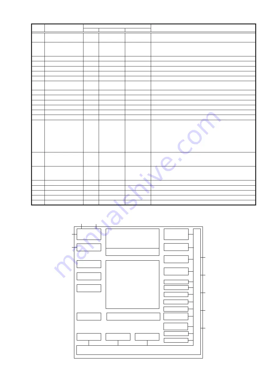
B oc  Di

r

1-CYCLE

80 1

CPU CORE

2 B SRAM

FLAS  CONTROLLER

32 B

FLAS  MEMORY

POWER 

MANA ER

LVD LVR

RESET

IOSC

CLOC

SELECT

WDT

XOSC

RTC

INTERRUPT

PORT0 1 2 3 4

UART-0 

PCA

ADC

TIMER0 1 2

IO MULTIPLEXER

VDD

VSS

RSTN

SPI

UART-1

I2C Master Slave

I2C Slave

VDD2

CEC EN INE

P As

PORT0  7:0

PORT1  7:0

PORT2  7:0

PORT3  7:0

PORT4  7:0

IO

 MU

LT

IPL

E

XER

Analog 

Comparators

Analog Switches

Summary of Contents for DBP-1611UD

Page 1: ...me illustrations using in this service manual are slightly different from the actual set Please use this service manual with referring to the operating instructions without fail For purposes of improvement specifications and design are subject to change without notice S0309 1V07DM D 1106 P e se refer to the MODIFICATION NOTICE ...

Page 2: ...portant safety parts that are indicated by the z mark on schematic diagrams and parts lists be sure to use the designated parts Be sure to mount parts and arrange the wires as they were originally placed For safety seasons some parts use tapes tubes or other insulating materials and some parts are mounted away from the surface of printed circuit boards Care is also taken with the positions of the ...

Page 3: ...ide film RW winding RN Metal film RK Metal mixture P Pulse resistant type NL Low noise type NB Non burning type FR Fuse resistor F Lead wire forming 2B 1 8 W 2E 1 4 W 2H 1 2 W 3A 1 W 3D 2 W 3F 3 W 3H 5 W F 1 G 2 J 5 K 10 M 20 Ex RN Type 14K Shape and per formance 2E Power 182 Resist ance G Allowable error FR Others Resistance 1800ohm 1 8kohm 1 8 2 Indicates number of zeros after effective number 2...

Page 4: ...tential Alle IC s en vele andere halfgeleiders zijn gevoelig voor elektrostatische ontladingen ESD Onzorgvuldig behandelen tijdens reparatie kan de levensduur drastisch doen verminderen Zorg ervoor dat u tijdens reparatie via een polsband met weerstand verbonden bent met apparaat Houd componenten en hulpmiddelen ook op ditzelfde potentiaal Tutti IC e parecchi semi conduttori sono sensibili alle sc...

Page 5: ...operly grounded to remove any static electricity that may be charged on the body 2 Ground for Workbench Be sure to place a conductive sheet or copper plate with proper grounding 1 M on the workbench or other surface where the semi conductors are to be placed Because the static electricity charge on clothing will not escape through the body grounding band be careful to avoid contacting semi conduct...

Page 6: ...ady Analog audio output Output level 2 Vrms 10 kΩ 2 channels output terminal Pin jack 1 set Audio output characteristics 1 Frequency response q BD Linear PCM 2Hz 22kHz 48kHz sampling 2Hz 44kHz 96kHz sampling 2Hz 88kHz 192kHz sampling w DVD Linear PCM 2Hz 22kHz 48kHz sampling 2Hz 44kHz 96kHz sampling 2Hz 88kHz 192kHz sampling e Super Audio CD 2Hz 40kHz r CD 2Hz 20kHz 2 S N ratio 115dB 3 Total harmo...

Page 7: ...LX 108 z Refer to MEASURIN MET OD AND WAVEFORMS When you repair the BD MEC A UNIT you can use the following I Please order to marant Official Service Distributor in your region if necessary Do not supply it 2 Dimensional Bar Code Reader DS6708 made by Symbol Co etc 1 Set Do not supply it 232C TTL USB conversion jig Model DUT 0663 by eeeTech 1 Set Part No 6120 000300AS 4P RE P CONN CORD 1000mm 1 Se...

Page 8: ...ut the shooting direction of each photograph Photographs with no shooting direction indicated were taken from the top of the set The ie point of e ch photo r ph Shootin direction View from the top Front side Shooting direction B Shooting direction D Shooting direction C Shooting direction A TOP COVER FRONT PANEL ASSY Refer to DISASSEMBLY 1 FRONT PANEL ASSY and EXPLODED VIEW FRONT PANEL ASSY Ref No...

Page 9: ...k the claw and move in the direction of arrow to gradually pull out the assembly Proceedin TOP COVER FRONT PANEL ASSY Shooting direction B 4 FFC cable Shooting direction D View from the bottom Shooting direction C Please refer to EXPLODED VIEW for the disassembly method of each P W B included in FRONT PANEL ASSY ...

Page 10: ...wires and FFC cables then remove the screws 2 Remove the screws 3 Remove the screw Proceedin TOP COVER FRONT PANEL ASSY BD MAIN UNIT ASSY BAC PANEL ASSY BD MAIN UNIT ASSY CN FFC cable POWER PWB UNIT FFC cable P2 Shooting direction A View from the bottom ...

Page 11: ...or the disassembly method of MAIN P W B included in BD MAIN UNIT Proceedin TOP COVER REMOTE PWB UNIT Please refer to EXPLODED VIEW for the disassembly method of IR PWB UNIT Proceedin TOP COVER FAN Please refer to EXPLODED VIEW for the disassembly method of FAN Proceedin TOP COVER FAN POWER PWB UNIT Please refer to EXPLODED VIEW for the disassembly method of POWER PWB UNIT ...

Page 12: ...12 REMOVING DISCS 1 Remove the Top Cover 2 Open the CD tray by turning the Drive gear counterclockwise Shooting direction D Drive gear ...

Page 13: ...ary after the replacement OW TO REPACE T E BD MAIN UNIT OR T E BD MEC A UNIT ASSY page 1 L ser dri e current initi ue FL Display The display part of 13 digits CD 1 2 3 4 6 7 8 9 10 11 12 13 T 2 1 m m m m n n n n FL Display The display part of 13 digits DVD 1 2 3 4 6 7 8 9 10 11 12 13 T 2 2 m m m m n n n n FL Display The display part of 13 digits BD SL 1 2 3 4 6 7 8 9 10 11 12 13 T 2 3 m m m m n n ...

Page 14: ... X m m m m n n n n X 1 CD laser mode 2 DVD laser mode 3 BD SL laser mode mmmm mA Initial value nnnn mA Current value 2 To c e r the ccu u ted ser on ti e Press the 1 button while the accumulated laser on time is displayed TC1 TC2 TC3 until TC4 clear appears at the display If the 1 button is pressed the accumulated laser on time of CD DVD and BD is cleared FL Display The display part of 13 digits 1...

Page 15: ...P1611 see DISASSEMBLY 2 Follow the firmware update procedure and update the firmware to the latest version see VERSION UP RADE PROCEDURE OF FIRMWARE 2 o to Rep ce the BD MEC A UNIT ASSY 2 1 De ices Used 1 PC 2 2 Dimensional Bar Code Reader DS6708 made by Symbol Co etc Do not supply 3 USB 232C TTL conversion jig Model DUT 0663 by eeeTech Do not supply 4 4P RE P CONN CORD 1000mm Part No 6120 000300A...

Page 16: ...on of the set before the BD MEC A UNIT ASSY is replaced 2 Decompress the D M ScanBarcode Rpower 2 16 60 ES460 MP function ip folder and start the Rpower e e 3 A pop up is displayed Click O 4 Click O PC USB へ MAIN PWB UNIT CON601 4P RE P CONN CORD 1000mm umper pin 3 3V f mark USB 232C TTL conversion sig View from the bottom 2 Dimensional Bar Code BD MEC A UNIT ASSY for replacement The 2 dimensional...

Page 17: ...17 On the screen below select ComPort XX Select the USB 232C TTL conversion jig port 6 Check Directly ...

Page 18: ...s finished reading the barcode the read data is displayed b If the 2 dimensional barcode data has already been read by the 2 dimensional barcode reader and the converted data obtained copy the data from the data file and paste it into this section NOTE Be sure not to ist e the i ht pic up b r code d t settin s ith d t fro different pic up Writin incorrect d t i c use ser de r d tion Click ...

Page 19: ...hen Pass changes to green writing to the Flash ROM of the MAIN PWB UNIT is complete 11 Switch off the set unit power and remove the 232C TTL side 4P P connector of the USB 232C TTL conversion jig from the MAIN PWB UNIT CON601 ...

Page 20: ...he set unit see DISASSEMBLY 2 Remove the MEC A COVER 3 Disconnect the connector wire and FFC cable 4 Move the optical pickup to the outer circumference remove the FFC Cable and remove the screws DRIVE MEC A UNIT TOP COVER A700 FFC cable MAIN PWB UNIT OPTICAL PIC UP FFC cable ...

Page 21: ... off mode in the test mode page 2 Check that the values are 6 mA from the initial value for BD and 12 mA from the initial value for DVD CD 2 Clear the total laser usage time see the procedure for clearing the accumulated laser on time in test mode page 26 3 Check BD DVD and CD media playback 4 If there are no problems with playback remove the disc press the ON STANDBY button to switch to standby s...

Page 22: ...INITIALI IN is displayed on the FL tube 3 The display on the FL tube switches to INITIALI ED the NO DISC display reappears and initiali ation is completed 2 Fir re ersion chec ode 2 1 prep r tion 1 E uipment used None 2 Unit setting No spec other than the following procedure 2 2 procedure b Front end and Back end and SYS com version check mode 1 Press the SETUP button on the remote controller to d...

Page 23: ...the FL tube and operations with the remote control and the REMOTE CONTROL input terminal on the back of the DBP 1611UD are disabled C nce 1 Pressing the PURE DIRECT and 3 buttons for simultaneously 2 Lock Off is displayed on the FL tube and remote lock mode is made canceled 5 A Lit A Off ode for the FL tube 5 1 prep r tion 1 E uipment used None 2 Unit setting No spec other than the following proce...

Page 24: ...No display mode T Test mode cancel TI q When the 9 button is pressed after entering the test mode the display switches in the order T2 T7 TC T TI T2 FL Display The display part of 13 digits 1 2 3 4 6 7 8 9 10 11 12 13 T 2 L a s e r O n O f f FL Display The display part of 13 digits 1 2 3 4 6 7 8 9 10 11 12 13 T 7 E r r o r R a t e FL Display The display part of 13 digits 1 2 3 4 6 7 8 9 10 11 12 1...

Page 25: ...ss the 1 button to begin error rate measurement The address and error rate are displayed For a description of the displayed measurement results see Table 1 Error rate details FL Display The display part of 13 digits 1 2 3 4 6 7 8 9 10 11 12 13 T Y Y m m m m m m l l l l YY selection mode 71 to 94 m address PBA EX l error rate COUNT SEC DEC Note CD 4 speed Renewal of data is carried out for every 30...

Page 26: ...ime of CD DVD and BD is cleared FL Display The display part of 13 digits 1 2 3 4 6 7 8 9 10 11 12 13 T C 1 0 h When TC1 TC2 or TC3 is selected with the 8 or 9 button mmmmmm is displayed as 0 so you can check 4 Picking up No display mode Press the 8 or 9 button to switch to the pickup number display The pickup number is a 1 digit number so it is displayed in two sections FL Display The display part...

Page 27: ...ayer It is invalid It is invalid C2 uncorrectable error number When this is selected for BD or DVD T74 FFFFFFFFFF display 7 The central circumference of 1 layer BIS error detection signed number It is invalid It is invalid When this is selected for DVD or CD T7 FFFFFFFFFF display 76 The central circumference of 1 layer It is invalid It is invalid It is invalid When this is selected for BD DVD or C...

Page 28: ...r It is invalid When this is selected for DVD 1 layer or CD T89 FFFFFFFFFF display 90 The central circumference of 2 layer It is invalid It is invalid It is invalid When this is selected for BD DVD or CD T90 FFFFFFFFFF display 91 The outer circumference of 1 layer BIS error detection signed number It is invalid It is invalid When this is selected for DVD or CD T91 FFFFFFFFFF display 92 The outer c...

Page 29: ...he firmware on the website is latest proceed to 4 If the latest firmware has been already installed press the 8 button to return to SETUP menu 4 Use the Cursor buttons to select Update then press the ENTER button When updating is completed return to normal status about 20 seconds later C utions on Fir re Upd te In order to update the firmware you must have the correct system re uirements and setti...

Page 30: ...and soldering 6 7 DTS114EUA U2 U7 PC817 and other circuits Check Ps On input P4 2 Press the ON STANDBY button to check Normally 3 3V is output O if 3 3V is output even momentarily Check parts surrounding and soldering P4 1 PIN FFC 1 0mm MAIN UNIT U16 CS8966F P FP447 and other circuits Check AC DET signal output P4 1 AC 0 0 Vp p AC60 60 Vp p Check parts surrounding and soldering D11 D12 IN4007 U4 P...

Page 31: ... 1 20 1 W OUSIN and other circuits Check parts surrounding and soldering U3 MR 662 UYB POWER UNIT T1 EER28 SW TRANS D19 FR307 1 20 1 W OUSIN and other circuits Check parts surrounding and soldering U PT6302 POWER UNIT T1 EER28 SW TRANS D4 FR107 1 20 1 W OUSIN and other circuits N G N G N G O O Check parts surrounding and soldering U PT6302 U3 MR 662 UYB 1 20 1 W OUSIN POWER UNIT P3 20PIN FFC 1 0mm...

Page 32: ...R 73 C32 861 Replace the MAIN UNIT 3 2 Component out doesn t output Check the input signal to U18 Y2 U18 10pin Y3 U18 14pin Y1 U18 16pin Check soldering U18 N M2 66AV and surrounding circuits C 41 C 42 C 43 R 80 R 87 R 88 R 91 R 92 R 9 N G O Check the output signal from U18 YOUT U18 23pin PBOUT U18 21pin PROUT U18 18pin Check the power supply and control signal for U18 V AV U18 3pin COMP MUTE U18 ...

Page 33: ...ck the digital input siginal for U802 AOMCL U802 pin Mater Clock AOSDATA0 U802 6pin Digital Data AOBC U802 7pin Bit Clock AOLRC U802 8pin LR Clock Replace the U802 Check the mute control signal and ERO Detect signal for U802 DAC ero Detect MUC AMUTE Low MT8 30 AMUTE Low U802 16pin Low Check soldering 21 D866 12 18 16 13 Check the audio output for U801 Lch U801 1pin Rch U801 7pin Check soldering U8...

Page 34: ...l FB861 Check the digital signal for 3Vpp Replace the MAIN UNIT Replace C868 R868 R866 211 R862 R864 R863 R869 3 Ether is not connection Check the input signal for U901 SMSC8710 Check the power supply voltage Replace the MAIN UNIT Check the POWER UNIT N G O Check the output signal for U901 SMSC8710 Replace the MAIN UNIT N G Check soldering for D23 P900 O N G N G O O ...

Page 35: ... Bar 100 Component output resolution 1080i It is better to use wires for e tending between the probe and test points Since there are no test points for locations q to r confirm the signals at the land of a chip resistor MAIN UNIT TEST POINT AND WAVEFORMS A Component side Det i A qU18 N M2 66 Video out signal w rU18 N M2 66 Component out Y Cb Cr signal 4 3 1 2 t ND qVideo out signal wComponent out ...

Page 36: ...n output chec Signal Color Bar 100 DBP 1611 Oscilloscope 7 ohm Load Video out terminal check Video out signal Component out terminal check Component out Y signal Component out Cb signal Component out Cr signal ...

Page 37: ...EC FL DRV 1 bits DDR2 SDRAM 8 bits NAND FLAS 1 bits DDR2 SDRAM 1 bits DDR2 SDRAM 1 bits DDR2 SDRAM 2 M SYS u com CS8966F IR REMO BE CONT ON ST POWER VIDEO DRIVER N M2 66AV COMPONENT OUT VIDEO OUT DMI OUT DI ITAL OUT AUDIO DAC PCM1781 MUTE OPAMP 2C AUDIO OUT 11 0 92 M EEPROM 10 100 Ethernet Transciever SMSC8710 ET ERNET 2 M POWER PWB FFC SMPS 12V P AC INLET Standby SMPS Sub Power to MAIN PWB to DIS...

Page 38: ...IN UNIT HA700 J700 HA600 JT10 DISPLAY UNIT STANDBY SW UNIT J2 J3 16P BtoB J4 POWER UNIT J405 J407 JP4 JP2 15P FFC P1 0 13P PH PH JP5 JP6 JP3 JP1 AC INLET 20P FFC P1 0 SUB POWER UNIT JP1 JP2 9P BtoB 14P BtoB CN5 J306 REMOTE UNIT J1 12P FFC P1 0 FAN 2P PH J1 WIRING DIAGRAM ...

Page 39: ... 2 1 I G F E D C B A 1 2 3 4 5 I G F E D C B A PRINTED WIRING BOARDS MAIN COMPONENT SIDE 鉛フリー半田 半田付けには 鉛フリー半田 Sn Ag Cu を使用してください Le d free So der When soldering use the Lead free Solder Sn Ag Cu MAIN FOIL SIDE ...

Page 40: ...11 1 5 4 3 2 1 G F E D C B A 14 13 12 11 1 5 4 3 2 1 D C B A 鉛フリー半田 半田付けには 鉛フリー半田 Sn Ag Cu を使用してください Le d free So der When soldering use the Lead free Solder Sn Ag Cu POWER COMPONENT SIDE DISPLAY COMPONENT SIDE ...

Page 41: ... 2 3 4 5 1 11 12 13 14 D C B A 1 2 3 4 5 1 11 12 13 G F E D C B A 鉛フリー半田 半田付けには 鉛フリー半田 Sn Ag Cu を使用してください Le d free So der When soldering use the Lead free Solder Sn Ag Cu DISPLAY FOIL SIDE POWER FOIL SIDE ...

Page 42: ... COMPONENT SIDE STANDBY SW COMPONENT SIDE SUB POWE COMPONENT SIDE 5 4 3 2 1 D C B A 5 4 3 2 1 C B A 4 3 2 1 C B A 1 2 3 4 C B A 1 2 3 4 5 C B A 1 2 3 4 5 D C B A 鉛フリー半田 半田付けには 鉛フリー半田 Sn Ag Cu を使用してください Le d free So der When soldering use the Lead free Solder Sn Ag Cu ...

Page 43: ...K R29 2K R11 2M R11 2M D9 FR107 D9 FR107 C27 2 2uF 50V C27 2 2uF 50V R19 120k R19 120k R37 27k R37 27k NC 2 S GND 3 VCC 4 SS OLP 5 FB 6 OCP BD 7 D 1 IC1 STR W6753 IC1 STR W6753 1 2 U6A PC817 U6A PC817 R7 1k R7 1k SF34 R35 0 R35 0 R17 47k R17 47k R43 2 2R 1 4W R43 2 2R 1 4W C65 0 1uF C65 0 1uF R28 220 R28 220 C11 NC C11 NC R5 2M R5 2M C44 0 1uF 50V C44 0 1uF 50V 4 8 6 15 16 11 10 2 13 14 9 12 T1 EE...

Page 44: ...8HS280NT C23 0 1u R12 100K C25 47 16 IC2 MP2208 AGND 1 SS 2 PGND1 3 SW 4 IN1 5 NC 6 BS 7 Vcc 8 POK 9 IN2 10 SW 11 PGND2 12 EN SYNC 13 FB 14 C22 0 01u C21 1000P C31 4 7u R13 100K L8 3 3uH C33 0 01u C27 0 01u L6 FBJ1608HS280NT R18 NC C28 0 1u Z DZ2 47V C32 4 7u C26 22 16 C24 47 16 R14 499K 1 R11 0 C36 22u IC4 NJM79M09DL1A 1 2 3 IC3 NJM7809DL1A 1 2 3 C18 C19 D1 1SS355 D2 1SS355 100 16V C20 100 16V C4...

Page 45: ...3 GR11 42 GR10 41 GR9 40 GR8 39 GR7 38 GR6 37 GR5 36 GR4 35 GR3 34 GR2 33 GR1 32 SG35 31 SG34 30 SG33 29 SG32 28 SG31 27 SG30 26 SG29 25 GR14 45 GR15 46 GR16 47 VEE 48 VSS 49 OSCI 50 OSCO 51 RSTB 52 CSB 53 CLKB 54 DIN 55 VDD 56 P1 57 P2 58 AD2 59 AD1 60 SG1 61 SG2 62 SG3 63 SG4 64 U5 PT6302 U5 PT6302 D3 NC D3 NC R25 39k 1 R25 39k 1 D4 NC D4 NC R13 10k NC R13 10k NC D1 NC D1 NC D2 NC D2 NC D7 BAT85...

Page 46: ...D5 OPEN 1 2 3 JK1 JK1 C7 220pF C7 220pF C23 0 1Z C23 0 1Z R25 R25 CE5 47uF 16v CE5 47uF 16v TP10 TP10 C15 1000pF C15 1000pF R26 R26 R3 1K R3 1K CE1 0 1 50V CE1 0 1 50V D1 RB521S D1 RB521S R2 3 3K R2 3 3K TP2 TP2 R27 0 R27 0 C9 0 01 C9 0 01 R4 10K R4 10K C24 0 1uF C1608 SMD C24 0 1uF C1608 SMD ZD4 OPEN ZD4 OPEN CE2 0 22 50V CE2 0 22 50V C19 OPEN C19 OPEN C10 OPEN C10 OPEN 3 1 2 4 W405 M3 SITE W405 ...

Page 47: ... R35 1K FB404 BLM15P FB404 BLM15P CE27 220uF 10v LESR CE27 220uF 10v LESR C15 22uF 10v C15 22uF 10v POR U19 G691L293T73U POR U19 G691L293T73U GND 1 RESET 3 VCC 2 R426 100 R426 100 R38 47K R38 47K C48 NC C48 NC R371 100 R371 100 CE13 220uF 16v CE13 220uF 16v C10 NC C10 NC FB20 BLM15P NC FB20 BLM15P NC R58 10K_1 R58 10K_1 FB24 BLM21P FB24 BLM21P C64 NC C64 NC CE4 100uF 10v CE4 100uF 10v FB403 BLM15P...

Page 48: ...M8 VDD M9 VSS N1 A3 N2 A5 N3 A6 N7 A4 N8 A7 P2 A9 P3 A11 P7 A8 P8 VSS P9 VDD R1 A12 R2 NC A14 R3 NC N15 R7 NC A13 R8 VDDQ G3 RN103 100x4 RN103 100x4 1 2 3 4 5 6 7 8 C148 0 1uF 16V C158 0 1uF 16V C158 0 1uF 16V C133 0 1uF 16V C133 0 1uF 16V C119 0 1uF 16V C119 0 1uF 16V C111 0 1uF 16V C111 0 1uF 16V C132 0 1uF 16V C132 0 1uF 16V C150 0 1uF 16V C150 0 1uF 16V RN102 100x4 RN102 100x4 1 2 3 4 5 6 7 8 ...

Page 49: ...DQ E9 DQ6 F1 VSSQ F2 LDM F3 LDQS F7 VSSQ F8 DQ7 F9 VDDQ G1 DQ1 G2 VDDQ G7 DQ0 G8 VDDQ G9 DQ4 H1 VSSQ H2 DQ3 H3 DQ2 H7 VSSQ H8 DQ5 H9 VDDL J1 VREF J2 VSS J3 VSSDL J7 CK J8 VDD J9 CKE K2 WE K3 RAS K7 CK K8 ODT K9 NC BA2 L1 BA0 L2 BA1 L3 CAS L7 CS L8 A10 AP M2 A1 M3 A2 M7 A0 M8 VDD M9 VSS N1 A3 N2 A5 N3 A6 N7 A4 N8 A7 P2 A9 P3 A11 P7 A8 P8 VSS P9 VDD R1 A12 R2 NC A14 R3 NC N15 R7 NC A13 R8 VDDQ G3 R2...

Page 50: ... NC C941 NC C941 NC C944 1uF C944 1uF FB209 BLM15P FB209 BLM15P C970 0 01uF C970 0 01uF C937 22pF C937 22pF U100C MT8530_DDR2 MT8530 BGA702 P0 695 B0 5 U100C MT8530_DDR2 MT8530 BGA702 P0 695 B0 5 AVDD33_VDACR E31 AVSS33_VDACR H32 AVDD33_VDACY G31 AVSS33_VDACY H30 AVDD33_VDACBG D32 AVSS33_VDACBG F32 AVDD33_XTAL E25 AVSS33_XTAL G25 AVDD33_XTAL25M BC7 AVSS33_XTAL25M AY8 AVDD33_SACD AU5 AVSS33_SACD AV...

Page 51: ...EST POINT SMD1 0 TP305 TP305 R1182 10K R1182 10K R300 10K R300 10K TP315 TEST POINT SMD1 0 TP315 TEST POINT SMD1 0 R308 10K R308 10K C318 0 01uF C318 0 01uF C307 0 1uF C307 0 1uF TP308 TEST POINT SMD1 0 TP308 TEST POINT SMD1 0 TP311 TEST POINT SMD1 0 TP311 TEST POINT SMD1 0 FB305 BLM15P FB305 BLM15P TP306 TP306 R1243 0R R1243 0R R312 10K R312 10K FB303 BLM15P FB303 BLM15P FB306 BLM18P FB306 BLM18P...

Page 52: ...UPG HW Trapping Pin Boot ICE 0402 For STBY MCU 232 VFD IR RS232 0402 VCC3IO_STB Below 20mA AVDD33_LDO Below 20mA CNT MII HW TRAPPING C406 0 1uF C406 0 1uF R404 10K R404 10K R413 10K NC R413 10K NC C402 0 1uF NC C402 0 1uF NC U100D MT8530_DDR2 MT8530 BGA702 P0 695 B0 5 U100D MT8530_DDR2 MT8530 BGA702 P0 695 B0 5 VCC3IO_STB J33 VCC3IO_STB G35 AVDD33_LDO J37 AVSS33_LDO K36 AVDD10_LDO H38 ETCOL C37 ET...

Page 53: ...A5 VOUTD6 D6 VOUTD7 B6 VOUTD8 C7 VOUTD9 A7 VOUTD10 B8 VOUTD11 C9 VOUTD12 A9 VOUTD13 D10 VOUTD14 B10 VOUTD15 C11 VOUTD16 E11 VOUTD17 F12 VOUTD18 G13 VOUTD19 E13 VINVSYNC E17 VINHSYNC B16 VINCLK D16 VIND0 A11 VIND1 D12 VIND2 E15 VIND3 F16 VIND4 B12 VIND5 F14 VIND6 H14 VIND7 F18 VIND8 G15 VIND9 J17 VIND10 G17 VIND11 C13 VIND12 A13 VIND13 D14 VIND14 B14 VIND15 C15 VIND16 A15 VIND17 D18 VIND18 G19 VIND...

Page 54: ...uF 16V TP745 TP745 NO600 C629 2200pF C629 2200pF C612 0 1uF C612 0 1uF TLSO TLSO C630 220pF C630 220pF C711 0 1uF C711 0 1uF C613 0 1uF C613 0 1uF R619 0R R619 0R TP742 TP742 TP751 TP751 TP719 TP719 FMSO3 FMSO3 R1028 0 R1028 0 CE691 220uF 10v CE691 220uF 10v R652 0 R652 0 TP721 TP721 U100G MT8530_DDR2 U100G MT8530_DDR2 FE_V14 U7 FE_VFVREF N5 FE_HAVC J1 FE_AGND W5 FE_TRINA P4 FE_TRINB R5 FE_TRINC N...

Page 55: ... GAINSW1 GAINSW1 FB704 BLM21P FB704 BLM21P B B C1019 NC C1019 NC R1035 0 R1035 0 C1026 NC C1026 NC C1023 NC C1023 NC R705 10K R705 10K FOC1 FOC1 B B U700 R2A30209SP SSOP42 SMD U700 R2A30209SP SSOP42 SMD SPIN 1 SL1IN 2 SL2IN 3 SPLIN 4 VM2 5 SL2 6 GND 7 SL2 8 SL1 9 SL1 10 GND 11 U 12 V 13 W 14 ACTFLG 15 COMMON 16 TEST 17 SLLIM 18 FG 19 EN1 20 EN2 21 REF 42 LOIN 41 FOIN 40 TOIN 39 TLIN 38 TL 37 TL 36...

Page 56: ...5 NC R135 NC D3 1SS301 D3 1SS301 1 3 2 L7 NC L7 NC C968 220pF 5 50V C968 220pF 5 50V R140 1K R140 1K Q25 KTC2875 Q25 KTC2875 1 3 2 Q16 DTC114EUA Q16 DTC114EUA 1 3 2 R78 33 R78 33 R79 0 R79 0 R132 47K_1 4W R132 47K_1 4W R966 8 2k R966 8 2k Q11 KTC2875 Q11 KTC2875 1 3 2 R957 39K R957 39K CE24 100uF 50v CE24 100uF 50v C24 15pF C24 15pF C540 10uF 16v C540 10uF 16v CE18 470uF 16v CE18 470uF 16v CB8 0 1...

Page 57: ...164 NC C164 NC C153 0 1uF C153 0 1uF FB861 BLM15A FB861 BLM15A P6 COAX P6 COAX 1 2 R592 75_1 R592 75_1 R864 3 9K R864 3 9K R562 0 R562 0 R576 0 R576 0 R591 75_1 R591 75_1 R575 0 R575 0 C180 NC C180 NC C182 NC C182 NC C163 NC C163 NC C541 10uF C541 10uF C166 NC C166 NC R581 10K R581 10K C543 10uF C543 10uF R573 75_1 R573 75_1 R588 75_1 R588 75_1 C478 0 1uF C478 0 1uF R868 68 R868 68 L82 22uH L82 22...

Page 58: ...NC R1022 0 NC C987 33PF C987 33PF R985 33 R985 33 R999 0 R999 0 R930 49 9 R930 49 9 C976 0 1uF C976 0 1uF R1006 10K R1006 10K C988 33PF C988 33PF R1017 10K NC R1017 10K NC R983 1 5K R983 1 5K C985 0 1uF C985 0 1uF C980 0 022uF 50V C980 0 022uF 50V R929 49 9 R929 49 9 R995 0 R995 0 C977 0 1uF C977 0 1uF R931 10 R931 10 R991 47 R991 47 R987 0 R987 0 R986 0 R986 0 R927 49 9 R927 49 9 R1001 0 R1001 0 ...

Page 59: ...82 33 R282 33 MCU_CEC_IN MCU_CEC_IN R256 100 R256 100 C69 0 1uF 16V C69 0 1uF 16V R382 47K R382 47K R258 33 R258 33 TXD_0 TXD_0 D205 1N4148 D205 1N4148 R218 NC R218 NC MCU_SCL MCU_SCL R281 NC R281 NC MCU_SDA MCU_SDA R129 47K R129 47K C184 1uF C184 1uF R287 33 R287 33 SPI_DO SPI_DO R349 NC R349 NC R344 33 R344 33 R351 R351 C178 100pF NC C178 100pF NC C62 0 1uF 16V C62 0 1uF 16V U304 GT24C02 2ZLI TR...

Page 60: ...EXPLODED VIEW f A B Parts marked with this symbol have critical characteristics Use ONLY replacement parts recommended by the manufacturer WARNING 印の部分は安全を維持するために重要 な部品です 従って交換時は必ず指定の 部品を使用してください 60 ...

Page 61: ... 972304000010S BD MAIN UNIT DBP1611 7025HV1002010 1 1 nsp MAIN PWB UNIT ASSY 1 11 963309100070S BD MECHA UNIT ASSY DBP1611 8038041669010S 1 67 nsp 9P FFC 1 0 N711091033810S 1 12 nsp MECHA BRACKET 4010215106100S 1 13 nsp DAMPER 60X10 4050213415000S 1 14 nsp DAMPER 40X35 4050213425000S 1 15 nsp DAMPER 75X35 4050213435000S 1 17 nsp HEAT SHEET 25X25 T1 5 1210211539000S 1 19 nsp HEAT SINK 2120211958000...

Page 62: ...KNOB 1611BK BK 5090214591000S 1 37 nsp OPEN CLOSE KNOB 1611SP SP 5090214591100S 1 38 nsp KNOB 1P 1611BK BK 5097214611000S 1 38 nsp KNOB 1P 1611SP SP 5097214611100S 1 39 nsp WINDOW 1611 5077213133000S 1 52 nsp BUFFER 10x150x10t 1 40 nsp EMIGASKET NLCG100100 15mm 4400210619000S 1 41 nsp ALUMINUM TAPE 35mm 1220210978000S 1 42 418510021006D LOADER PANEL 1611BK BK 4317215341000S 1 42 418510021013D LOAD...

Page 63: ...2641000080S AC INLET AC M34U E3 G430341535510S 1 z JP1 972641000510S AC INLET AC M34 E2 E2R EA E1C E1 G430040600020S 1 REMOTE PWB UNIT Ref No 3 JK1 00D2048729008 2P MINI JACK HSJ1003 016010WA G401HSJI05500S 1 KEY PWB UNIT Ref No 4 J3 645010079000S 16P PLUG P 2 54mm FEMALE HEADER SIDE L109000164540S 1 K1 K4 00MSP01010970 TACT SW KHH10910 H 5MM G180660065510S 1 LED1 00D3939671002 SMLU12416W S K50005...

Page 64: ...64 PACKING VIEW dfh 1 3 4 5 6 8 9 11121314 15 16 17 18 20 19 18 17 19 7 9 10 16 ...

Page 65: ... E1 EA 5227000002030S 1 7 nsp ADDENDUM SHEET 3D FOR E2 E2 5227000002040S 1 7 nsp ADDENDUM SHEET 3D FOR OTHER E2R E1C K 5227000002050S 1 8 nsp CABINET COVER 6327040022012S 1 9 972532000470D CUSHION 2012 L R 6230213024000S 1 10 nsp POLY COVER 6337040062010S 1 z 11 972611000410S AC CORD 2000mm UL 7A 125V E3 L068125075550S 1 z 11 972611000420S AC CORD 1500mm CB 2 5A 250V E2 E2R E1 L068250250440S 1 z 1...

Page 66: ... Crystal OUT for RTC oscillator 16 MCU SET3 I igh 3 3V or Low 0V igh 3 3V or Low 0V MCU setting pin by e ternail resistance Default is high 17 MCU AMUTE O Low 0V igh 3 3V Muting signal for audio output igh is for muting and Low is muting off 18 DMI POWER CTRL O Low 0V igh 3 3V Power enable is for the DMI V power supply igh is for DMI work normal And low is for DMI off 19 V MUTE O igh 3 3V i 0V Mut...

Page 67: ...U LED CTRL A O igh 3 3V Low 0V Control signal for Power On LED indication with reen color For the blink condition 1 reen Led blink at 1sec intervals between power on and boot The LED keep the light after the boot finishing 2 reen Led blink at 1sec intervals before the system becomes Standby compeletely when the power key is pressed in power on mode 38 MCU LED CTRL B O Low 0V igh 3 3V Control signa...

Page 68: ...u o r o t a l l i c s O O O C S O RSTB I Reset input pin When this pin is set to LOW all functions are initiali ed 2 CSB I Chip select input pin When this pin is set to igh Level the serial data transfer is disabled 3 CL B I Shift clock input pin The serial data is shifted at the rising edge of CL B 4 n i p t u p n i a t a d l a i r e S I N I D 6 y l p p u s r e w o p e v i t i s o P D D V 8 7 n i...

Page 69: ...69 MT 53 M in UNIT U1 B oc Di r MT8 30 OPU Motor Driver FLAS DRAM Audio DAC DMI CVBS Component Ethernet USB 2 0 ...

Page 70: ...k input 1 TEST 9 Test pin for factory use Must be LOW or open 1 2 VCC 11 Power supply V VCOM 13 Common voltage decoupling VOUTL 1 O Analog output for L channel VOUTR 14 O Analog output for R channel EROA 16 O ero flag output for L and R channels 1 Schmitt trigger input 2 Pulldown Po er Supp Enh nced Mu ti e e De t Si Modu tor VOUTL 4 O ers p in Di it Fi ter With Function Contro Audio Seri Port BC ...

Page 71: ...71 SMSC 1 M in UNIT U 1 B oc Di r ...

Page 72: ...72 N M25 AV M in UNIT U1 B oc Di r ...

Page 73: ...73 2 FL DISPLAY FL TUBE 15 BT 114GN Disp UNIT U3 ...

Page 74: ...74 Personal notes ...

Reviews: