background image

81

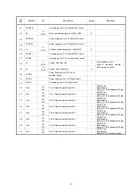
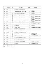
Pin

No.

Symbol 

I/O 

Description 

Default

Remarks

41

DVSS3R 

Grounding pin for 3.3V Muiti-Bit DAC circuit 

42

Ro

O

3AI/F

R channel audio output pin of Audio DAC. 

43

DVDD3R 

Power supply pin for 3.3V Audio DAC circuit. 

44

DVDD3L 

Power supply pin for 3.3V Audio DAC circuit. 

45

Lo

O

3AI/F

L channel audio output pin of Audio DAC 

46

DVSS3L 

Grounding pin for 3.3V Muiti-Bit DAC Circuit 


47

XVSS3 

Grounding pin for 3.3V clock oscillator circuit 


48

Xi

I

3AI/F

System clock Input pin 

49

Xo

O

3AI/F

System clock Output pin 

Xtal oscillation circuit. 

Connect 

feedback 

resistor 

M

:

between Xo and Xi 

50

XVDD3 

Power Supply pin for 3.3V clock 

oscillator circuit 

-

51

VDD1-2 

Power Supply pin for 1.5V Digital circuit 

52

VSS-2 

Grounding pin for 1.5V digital circuit 

53

Pio0

I/O

3I/F

Port 0

General Input/Output Port 


CMOS Port   
Schmitt input 
Refer to [1.2 Pin Assinment Table]

54

Pio1

I/O

3I/F

Port 1

General Input/Output Port 


CMOS Port 
Schmitt input 
Refer to [1.2 Pin Assinment Table]

55

Pio2

I/O

3I/F

Port 2

General Input/Output Port 


CMOS Port 
Schmitt input 
Refer to [1.2 Pin Assinment Table]

56

Pio3

I/O

3I/F

Port 3

General Input/Output Port 


CMOS Port 
Schmitt input 
Refer to [1.2 Pin Assinment Table]

57

Pio4

I/O

3I/F

Port 4

General Input/Output Port 


CMOS Port 
Schmitt input 
Refer to [1.2 Pin Assinment Table]

58

Pio5

I/O

3I/F

Port 5

General Input/Output Port 


CMOS Port 
Schmitt input 
Refer to [1.2 Pin Assinment Table]

59

Pio6

I/O

3I/F

Port 6

General Input/Output Port


CMOS Port 
Schmitt input 
Refer to [1.2 Pin Assinment Table]

60

Pio7

I/O

3I/F

Port 7

General Input/Output Port 


CMOS Port 
Schmitt input 
Refer to [1.2 Pin Assinment Table] 

Summary of Contents for DCD-520AE

Page 1: ...JP E3 E2 E1 E1C EA E2R EUT DCD 720AE P P DCD 520AE P P CD PLAYER Ver 1 S0444 1V01DM DG1205 Some illustrations using in this service manual are slightly different from the actual set Please use this s...

Page 2: ...LACED WITH A NEW ONE 27 PROCEDURE FOR UPGRADING THE VERSION OF THE FIRMWARE 27 1 Update for IC11 TMPM330FWFG 28 2 Update for IC41 TMP92FD28AFG USB com 32 TROUBLE SHOOTING 40 FLOW CHART NO 1 40 FLOW CH...

Page 3: ...arch for a Ref No in schematic diagrams printed wiring board diagrams block diagrams and parts lists 1 Press Ctrl Shift F on the keyboard The Search window appears Ctrl Shift F 2 Enter the Ref No you...

Page 4: ...ing Adobe Reader 9 On the Document menu click Sign Magnify schematic printed wiring board diagrams 1 Ctrl Space mouse operation Press Ctrl Space on the keyboard and drag the mouse to select the area y...

Page 5: ...reen Example using Adobe Reader 9 On the Tools menu point to Select Zoom and then click Pan Zoom Window Magnify schematic printed wiring board diagrams 3 Loupe Tool function The Loupe Tool function le...

Page 6: ...rtant safety parts that are indicated by the z mark on schematic diagrams and parts lists be sure to use the designated parts Be sure to mount parts and arrange the wires as they were originally place...

Page 7: ...THERWISE INDICATED P INDICATES MICRO MICRO FARAD EACH VOLTAGE AND CURRENT ARE MEASURED AT NO SIGNAL INPUT CONDITION CIRCUIT AND PARTS ARE SUBJECT TO CHANGE WITHOUT PRIOR NOTICE Parts indicated by nsp...

Page 8: ...s Sie im Reparaturfall dem Massepotential des Ger tes verbunden sind Halten Sie Bauteile und Hilfsmittel ebenfalls ber ein Pulsarmband mit Widerstand mit auf diesem Potential Alle IC s en vele andere...

Page 9: ...perly grounded to remove any static electricity that may be charged on the body 2 Ground for Workbench Be sure to place a conductive sheet or copper plate with proper grounding 1 M on the workbench or...

Page 10: ...le limits Below measurable limits Output level 2 0 V 10 k 2 0 V 10 k Signal type 16 bit linear PCM 16 bit linear PCM Sampling frequency 44 1 kHz 44 1 kHz Usable discs Compact Disc Compact Disc Digital...

Page 11: ...simultaneously while pressing 1 3 and 8 buttons 3 INITIALIZING is displayed on the FL tube Service Jig When you update the irmware by DFW you can use the following JIG RS232C to internal connector con...

Page 12: ...ism prior to anchoring in the set should be protected against static electricity and dust The mechanism must be stored that damaging outside forces are not received When carrying the inished mechanism...

Page 13: ...EMBLY 3 RADIATOR ASSY and EXPLODED VIEW CD MECHANISM ASSY Ref No of EXPLODED VIEW C9 DAC ASSY Refer to EXPLODED VIEW DAC PCB Ref No of EXPLODED VIEW C16 JOINT ASSY Refer to EXPLODED VIEW JOINT PCB Ref...

Page 14: ...graph Photographs with no shooting direction indicated were taken from the top of the set The photograph is DCD 720AE DCD 520AE model The viewpoint of each photograph Shooting direction View from the...

Page 15: ...15 1 MAIN ASSY 1 Remove the screws and disconnect the FFC Disconnect the connector wires CABINET TOP MAIN ASSY Proceeding PFCJ PFCK PFCI CN22 FFC CWC6 CWCN...

Page 16: ...cs 2 Remove the door by pulling 3 Remove the screws CABINET TOP FRONT PANEL ASSY Proceeding Shooting direction B View from the bottom Slide the projecting part located about 5cm inside in the directio...

Page 17: ...s 3 CD MECHANISM ASSY 1 Disconnect the connector wires then remove the screws CWP1 FFC CWCN CWJL CWPB cut cut CABINET TOP FRONT PANEL ASSY CD MECHANISM ASSY Proceeding CWC6 CWC7 Please refer to EXPLOD...

Page 18: ...18 4 AUDIO POWER ASSY 1 Remove the screws and disconnect the FFC Disconnect the connector wires AUDIO POWER ASSY JOINT ASSY CABINET TOP REAR PANEL DAC ASSY MAIN ASSY Proceeding CWJL CWPB Snap off...

Page 19: ...e 2 5 All displays on the FL tube lash every 2 seconds 3 Cold start mode 8 1 3 Initializing CD Player 4 CD test mode 8 5 Test of CD mech 5 CD heart run mode 9 1 3 Heat run mode 6 Laser on time 9 5 Las...

Page 20: ...SB microcomputer version 2 VFD check mode Turn off the power pressing Power operation button Press Power operation button while simultaneously while pressing 2 and 5 buttons To exit turn off All displ...

Page 21: ...n is pressed 4 STOP Servo 2 5 All servo on 2 5 6 Adjustment value display 2 After All servo on state FOCUS BALANCE 9 FOCUS GAIN 9 TRACKING BALANCE 9 TRACKING GAIN 9 FOCUS OFFSET 9 TRACKING OFFSET 9 RF...

Page 22: ...stop mode pickup moves in REV inwards or FWD outwards direction when 8 or 9 button pressed When 8 button pressed move to stop operation after detection that inner switch has turned on Pickup movement...

Page 23: ...current value is measured 3 seconds after the laser turns on The current value is updated every 3 seconds Press the 2 button return to CD test mode Stored data is not cleared even when the unit is Ini...

Page 24: ...all tracks If disc has 21 or more tracks skip to inal track after playback of irst track has inished e After disc playback has inished move pickup to innermost position and open tray r When loader op...

Page 25: ...ied time E3 01 PVD SVD analysis could not be completed within speciied time E4 04 Search time out E4 05 Error in communications with CD decoder E5 00 Inner switch not on E6 00 Inner switch not off E9...

Page 26: ...on the top line reappears Initialization of a count value is performed upon shipment from the factory and when the mechanism is replaced 7 Main com version up mode Turn on the power pressing Power op...

Page 27: ...hould write the new software on the microprocessor or lash ROM Please check the software version C Empty Flash ROM Without software You should write the software on the microprocessor or lash ROM Refe...

Page 28: ...1 Connection of SPK 581 PC and the unit See Connect SPK 581 Page 27 2 Turn on the unit 3 Double click BootTool_M330 and launch the Boot Tool_M330 4 Choose the Serial port number in the COM Port Turn...

Page 29: ...29 5 If successful communication between PC from the unit Connected will be displayed 6 Click Ram File button Then choose the OnBoard_M330 s32 Click Open button...

Page 30: ...30 7 Click Flash File Choose the Hex File S32 Choose the DCD720AE_20120404 01 s32 Click Open button 8 Click Start button...

Page 31: ...isconnect FFC of connection JIG from the unit 10 Initializing the unit Turn off the power button Press Power operation button while simultaneously while pressing 1 3 and 8 buttons 11 After updating th...

Page 32: ...Prepare the windows PC that installed the FlashProg EXE 2 Connection of SPK 581 PC and the unit See Connect SPK 581 Page 27 3 Double click FlashProg exe and launch the FlashProgrammer 4 Click the Setu...

Page 33: ...33 5 Click Device tab 6 Choose the TMP91FD28 in the Device and choose the 900 H1 in the Series Click Apply and display the chosen Dvice...

Page 34: ...34 7 Click Password 8 Choose the Device is Blank And Click OK...

Page 35: ...35 9 Click Object File tab 10 Click Browse...

Page 36: ...Choose the Motorola S Format s16 s24 s32 in Files of type Choose the BOLERO_ver014 s24 and click Open 12 The place of the ile is displayed Bolero_USB 20120330 01 Bolero_USB 2012033 1 Bolero_USB 20120...

Page 37: ...37 13 Click Option 14 Choose Erase Without Password for 900 Family And Click OK...

Page 38: ...cation tab 16 Choose the Serial port number in the COM Port Check the Data Rate Manual and input 9 in the Clock And Click OK The setting is completed Choose the Serial port that connect with 232C cabl...

Page 39: ...gue box saying Erase All data in this devise Y N appears automatically If the connection fails error message will appear Ex E000 Click Yes 19 Click A Auto Programing to start writing 20 Turn off the u...

Page 40: ...ective Check each voltage regulator circuit and service it if defective Is USB 5V voltage supplied to Pin 3 of IC22 Check if there is any leak or short circuiting rectiier circuit of SUB Power transfo...

Page 41: ...ng each switches S701 706 do the voltage of pin 91 92 of IC11 decrease Is approximately 42V voltage supplied to the kathode of D973 Are the contact point and the installation state of the key switches...

Page 42: ...ot be opened and closed Refer to FLOW CHART NO 9 The disc tray cannot be opened and closed Is the normal control voltage inputted to Pin 92 of IC11 Refer to FLOW CHART NO 6 The key operation is not fu...

Page 43: ...tive IC11 Pin 17 F_MUTE H mute L play Check AUDIO V 6V_A and AUDIO V 6V_A line and service it if defective DSP IC21 Check the DAC in DCD720AE IC64 DAC in DCD520AE IC65 digital audio data signal of a D...

Page 44: ......

Page 45: ......

Page 46: ...RN 1 1 CD TCD 784 Play 2 DISC DETECTION 2 1 CD TCD 784 DISC DETECTION 2 2 CD R TCD R000RM DISC DETECT 2 3 CD RW TCD W000RM DISC DETECTION 1V 200mV 2V 500Mv 2V 1V 2V RFO FSMONIT FOO TEI TRO FMO DMO 1V...

Page 47: ...MENT 3 TOC READ 4 FOCUS ADJUSTMENT 3 1 CD TCD 784 TOC READ 5 LOADER OPEN CLOSE 4 1 CD TCD 784 FOCUS ADJUSTMENT 1V 200mV 2V 500Mv 2V 1V 2V 1V 200mV 2V 500Mv 2V 1V 2V 1V 200mV 2V 500Mv 2V 1V 2V 5V 5V 5V...

Page 48: ...48 Personal notes...

Page 49: ...TOSHIBA USB JACK I2S AUDIO DAC TI DCD720AE PCM5142 BCK LRCK DATA OP AMP NJM2068 OP AMP NJM4556AL HEADPHONE AUDIO OUT OPTICAL OUT SPDIF OUT AUDIO L AUDIO R JRC JRC IPHONE FOO FMO CD MECHANISM KOTY CFL1...

Page 50: ...7 1 PMPC PMAD CWP3 CWP4 CWPB 3 1 3 1 CBLG CWFG JOINT PCB CUP12470Z 8 9 1 CWJL 9 1 1 6 1 5 6 1 5 1 CWC7 CWC6 FFC 16P FCFH FFC 15P FCCH 1 17 27 1 PFJC PFJD 27 1 PFJD 27 1 PFJD 1 17 PFJC 1 17 PFJC 1 9 PF...

Page 51: ...IC71 NJM4556AL DCD720AE Only 20dB Analog Signal Headphone Analog Signal Line Out 10dB Digital Signal I2S 5dB 6dB DAC GAIN L OUT 2 0V 0dB 2V 6dB 9 5dB R OUT 2 0V 6dB 10dB PHONES 1 1V HP AMP GAIN 32ohm...

Page 52: ...729 S704 S703 S702 S701 S706 S705 C754 CWFG JW04 R721 R725 R723 CWFB FCFH R716 R743 R742 R741 D723 D724 D725 D726 D727 D728 C741 C742 R744 R745 R722 C791 J722 J715 J702 J712 J713 J703 J718 J723 J724 J...

Page 53: ...Q773 Q774 D781 D782 C783 C784 L704 L703 L701 L702 C799 C798 R798 R799 Pb 1 GND 2 MCK BN22 AUDIO DAC DCD520AE PCM5102 DCD720AE PCM5142 16 9344MHz SCK FROM CD PCB BK23 CUP12470Z 7 DAC PCB D X601 PFDF C...

Page 54: ...R825 R826 R823 R824 PMAD PMAF CN83 CN82 D921 ET93 J908 J907 R882 R881 R802 R803 R809 R808 R807 R801 R806 J910 D909 D917 D916 D913 D907 R862 C881 J903 R805 R804 J901 CN21 PMAE R841 R842 C551 C552 C553...

Page 55: ...U CUP12470Z 4 C601 C603 JK61 CBUM BK21 L601 C604 C602 R601 D601 D602 D603 D604 C605 C606 L602 L603 2 GND CUP12470Z 3 LED PCB L D711 CBLG 3 R 1 G BK34 BK33 BK31 HP PCB MECHA CUP12470Z 8 JOINT PCB J PM...

Page 56: ...1 C204 C207 C209 C210 C212 C218 C222 C224 C225 C229 C230 C232 C233 C234 C237 C240 C244 C248 C250 C251 C254 C307 C401 C402 C407 C408 C415 C417 C420 C421 C433 C205 C215 C418 C202 C206 R411 R413 R160 P4...

Page 57: ...R983 22K D982 1SS355T Q981 RT1N141C D981 1SS355T D983 1SS355T R986 10K R988 47K D984 1SS355T R987 8 2K R984 100K R985 100K R989 1K R990 100K D985 1SS355T Q982 RT1N141C D919 1SS133MT 1 2 3 4 5 6 7 8 9...

Page 58: ...34 100P C735 100P C736 0 1uF R727 33 R729 33 R728 33 S704 SKIP R744 10K R743 1K R742 1 5K R741 1 8K S703 SKIP S702 STOP S701 CD USB C741 0 1uF R716 1K S706 OP CL S705 PLAY PAUSE C742 0 1uF C754 47 25V...

Page 59: ...R315 0 R208 0 R225 0 R226 0 R232 OPEN R233 OPEN R234 OPEN R235 OPEN R207 0 R312 18K R313 18K R314 18K C211 470 16V 1 2 3 4 5 6 CWC6 C324 0 1uF R316 0 100 99 98 97 96 95 94 93 92 91 90 89 88 87 86 85...

Page 60: ...P8 S5 x4 P6 P5 x4 x4 S2 x2 P12 x3 S1 S8 x5 x4 S3 x2 S3 x5 S3 S3 P1 x2 P13 x3 P1 1 P1 2 S1 S7 x3 x4 P2 P4 P3 S6 S10 x2 S3 S5 P11 P10 S11 P9 S5 x2 S2 S6 P14 x2 P16 P15 x2 P17 P18 x2 x6 M5 z z EXPLODED V...

Page 61: ...x4 x4 S2 x2 P11 x3 S1 S8 x5 x4 S3 x2 S3 x5 P1 x2 P12 x3 S1 S7 x3 x4 P4 P3 S10 x2 S5 P10 P9 P2 P7 P13 S5 x2 Delet P14 x2 P16 P17 x2 C7 C6 C4 C5 C8 C2 C3 C1 C11 C13 z z EXPLODED VIEW DCD520AE Parts mar...

Page 62: ...62 EXPLODED VIEW OF CD MECHANISM UNIT Parts marked with this symbol have critical characteristics Use ONLY replacement parts recommended by the manufacturer WARNING...

Page 63: ...1 943443100570D PANEL INNER BK CGW1A525B28 1 P1 1 nsp KNOB GUIDE CGW1A525 1 1 P1 2 nsp KNOB GUIDE CGW1A525 2 1 P17 00D9430189903 LENS CGL1A254 1 M2 42141002300AD BADGE DENON SP CGB1A254Y 1 M2 42141002...

Page 64: ...1A1115Y 1 nsp STICKER USB DCD720 CQB1A1116Z 1 nsp LABEL SERIAL NO CQB1A622 1 nsp CLAMPER ARM CHE154 nsp WIRE ASS Y 5P 100MM MECHA CWB2B005100GG 1 nsp WIRE ASS Y 6P 100MM MECHA CWB5A906100GG 1 94360650...

Page 65: ...89903 LENS CGL1A254 1 M2 42141002300AD BADGE DENON SP CGB1A254Y 1 M2 42141002301AD BADGE DENON BK CGB1A254Z 1 M9 00D9430179609 KNOB POWER SP CGK1A124YA 1 M9 00D9430179502 KNOB POWER BK CGK1A124ZA 1 P3...

Page 66: ...CHA CWB2B005100GG 1 nsp WIRE ASS Y 6P 100MM MECHA CWB5A906100GG 1 943606501570D CABLE CARD 15P 100MM A TYPE CWC4F4A15A100A10 1 943606007430S CABLE CARD CD Mecha 16P 1mm 100mm A TYPE CWC4F1A16A100A10 1...

Page 67: ...T690100300 1 4 943302100140D CD MECHANISM DA11VF 1 5 nsp INSULATOR KT690400600 4 6 nsp SCREW KT690400800 4 7 nsp SCREW KT628400400 1 8 nsp WAFFR 5PIN KT628300400 1 9 nsp PCB KT656300200 1 10 nsp SWITC...

Page 68: ...sp BAG POLY CPB1A013Y 1 3 00D9430177902 PAD SNOW CPS1A748 1 4 00D9430178008 PAD SNOW CPS1A749 1 5 1 943307006790D REMOCON TRANSMITTER ASS Y RC 1173 CARTDCD720A1 1 5 2 nsp BATTERY AAA 2PCS IN PACK CABR...

Page 69: ...UT CARTON CPG2A819N 1 2 nsp BAG POLY CPB1A013Y 1 3 00D9430177902 PAD SNOW CPS1A748 1 4 00D9430178008 PAD SNOW CPS1A749 1 5 1 943307006790D REMOCON TRANSMITTER ASS Y RC 1173 CARTDCD720A1 1 5 2 nsp BATT...

Page 70: ...ER_PROT I I L H POWER protect detect 3 AVSS A D converter GND pin 0V G G 4 VREFH Reference power supply P P 5 AVCC A D converter with a power supply P P 6 PG3 INT4 INT4 REMOTE_IN_1 I O I remote in 7 P...

Page 71: ...L E C T DCD520 ONLY I2S L L E F T J U S T I F I E D H DAC Input dara for SPI DCD720 ONLY 29 PB3 N C DAC_DEMP DCD520 ONLY DAC_MC DCD720 ONLY I O O L D A C D E E M P H A S I S C O N T R O L D C D 5 2 0...

Page 72: ...PA7 VFD_CLK I O O L L vfd clock 70 PJ0 INT0 INT0 EX_INTERRUT I O I H L External Interrupt Key 71 CVCC Power supply pin P P 72 X2 high speed oscillator Output oscillator 10MHz 73 CVSS GND pin G G GND...

Page 73: ...DCD 720AE I O use Note use NoUse init stby Act 97 PD2 AN6 PD2 Model Option I I Model Option DCD 720 LOW DCD 520 HIGH 98 PD3 AN7 AN7 LD_CHK I I A D mA 99 PD4 AN8 N C I I OPEN 10K Pull Down 100 PD5 AN9...

Page 74: ...74 TMP92CD28AFG IC41...

Page 75: ...75 TMP92CD28AFG Block Diagram...

Page 76: ...BOL I O O L L H when update control power on 25 P07 N C I O O Open L 26 DVSS3A DVSS3A 27 DVCC3A VDD3 3V 28 P10 MODEL OPTION I O I L L H or L RCD M39 LOW RCD M39DAB HIGH 29 P11 MODEL OPTION I O I L L H...

Page 77: ...N C O O Open L 71 P83 LRCK1 I O O L L H L 72 AM1 VDD3 3V 73 X2 X2 74 DVSS GND 75 X1 X1 76 DVCC3A VDD3 3V 77 P75 USB_OC I O I Open L USB Limit IC FLAG 78 P76 USB_EN I O O L L H USB Limit IC EN 79 D USB...

Page 78: ...78 TC94A92FG IC21...

Page 79: ...RFi I 3AI F RF signal input pin I Selectable Zin 20 10 k 5 RFRPi I 3AI F I 6 RFEQo O 3AI F O Connect to RFRPi by 0 1uF to RFi by 4700pF 7 DCoFC O 3AI F RFEQo offset compensation LPF output O Connect t...

Page 80: ...ut Port I CMOS Port Schmitt input Refer to 1 2 Pin Assinment Table 34 Pio9 I O 3I F Port 9 General Input Output Port I CMOS Port Schmitt input Refer to 1 2 Pin Assinment Table 35 Pio10 I O 3I F Port 1...

Page 81: ...rounding pin for 1 5V digital circuit 53 Pio0 I O 3I F Port 0 General Input Output Port I CMOS Port Schmitt input Refer to 1 2 Pin Assinment Table 54 Pio1 I O 3I F Port 1 General Input Output Port I C...

Page 82: ...3I F Microprocessor I F chip enable input pin I Schmitt input Refer to 1 2 Pin Assinment Table 68 MS I 3I F Microprocessor I F mode selection pin H Parallel I F L Serial I F I Refer to 1 2 Pin Assinm...

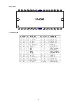
Page 83: ...O REGULATOR OUTPUT 7 MUTE I MUTE INPUT 8 SGND SIGNAL GROUND 9 FWD I CH5 INPUT 1 10 IN2 I CH2 INPUT 11 DO2 O CH2 OUTPUT 12 DO2 O CH2 OUTPUT 13 PGND1 POWER GROUND 1 14 REV I CH5 INPUT 2 NO SYMBOL I O D...

Page 84: ...26 25 24 23 22 28 DO1 DO1 IN1 IN1A N C REO MUTE SGND FWD IN2 DO2 DO2 PGND1 REV TSD 10K 10K D D Level Shift 10K 10K D D Level Shift IN2 10K 10K D D Level Shift D D SWITCH Level Shift MSC 10K 10K D D L...

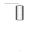
Page 85: ...CM514X PCM512X TOP VIEW DVDD 28 DGND 27 LDOO 26 XSMT 25 MISO 24 LRCK 23 DIN 22 BCK 21 SCK 20 GPIO6 19 1 CPVDD 2 CAPP 3 CPGND 4 CAPM 5 VNEG 6 OUTL 7 OUTR 8 AVDD 9 AGND 10 VCOM MS 18 MODE1 17 GPIO2 16 G...

Page 86: ...ut and output port GPIO4 14 I O General purpose digital input and output port GPIO3 15 I O General purpose digital input and output port GPIO2 16 I O General purpose digital input and output port MODE...

Page 87: ...nalog output from DAC right channel AVDD 8 Analog power supply 3 3V AGND 9 Analog ground DEMP 10 I De emphasis control for 44 1kHz sampling rate 1 Off Low On High FLT 11 I Filter select Normal latency...

Page 88: ...88 2 FL DISPLAY V F D FUTABA 16ST103GINK F701 PIN CONNECTION 1 43...

Page 89: ...MMBT5551 Q905 963216500060S T R RT1N144C 10K 47K CVTRT1N144C Q971 943219006820S TR KTC1027Y CVTKTC1027YT Q981 983 943216500020S T R RT1N141C 10K 10K CVTRT1N141C D601 603 00D2760717903 DIODE CHIP SWITC...

Page 90: ...1 5W 15Kohm J CRD20TJ153T R777 778 nsp RES CARBON 1 5W 47Kohm J CRD20TJ473T R779 780 nsp RES CARBON 1 5W 75ohm J CRD20TJ750T R781 782 nsp RES CARBON 1 5W 22Kohm J CRD20TJ223T R783 784 nsp RES CHIP 160...

Page 91: ...050059238S CAP ELECT ELNA RFG 50V 220uF 85 C 10X16 CCEA1HRFY221E C662 nsp CAP CHIP 1608 50V 0 1uF CCUS1H104KC C663 664 nsp CAP CHIP 1608 50V 15pF CCUS1H150JA C668 nsp CAP CHIP 2012 10V 2 2uF CCUC1A225...

Page 92: ...C956 957 nsp CAP CHIP 1608 50V 0 1uF CCUS1H104KC C958 00D2544749715 CAP ELECT 1000uF 25V RFO 12 5X20 CCEA1ERFO102E C959 nsp CAP CHIP 1608 50V 0 01uF CCUS1H103KC C961 962 nsp CAP CHIP 1608 50V 0 1uF CC...

Page 93: ...ANGLE B TO B P CJP17HJ282Z PFJD nsp PIN SOCKET 27P 1 25mm ANGLE B TO B CJP27HJ282Z PMAD nsp PIN HEADER 27P 1 25mm STRAIGHT B TO B CJP27GI281Z PMAE nsp PIN HEADER 13P 1 25mm STRAIGHT B TO B CJP13GI281Z...

Page 94: ...T D107 90M HD201820R DIODE SCHOTTKEY BARRIER HVDRB160L60TE25 D108 00D2760717903 DIODE CHIP SWITCHING 1SS355T HVD1SS355T D109 110 90M HD201820R DIODE SCHOTTKEY BARRIER HVDRB160L60TE25 D151 00D276071790...

Page 95: ...314 nsp RES CHIP 1608 5 18Kohm CRJ10DJ183T R315 316 nsp RES CHIP 1608 5 0ohm CRJ10DJ0R0T R401 404 nsp RES CHIP 1608 5 33ohm CRJ10DJ330T R407 nsp RES CHIP 1608 5 22Kohm CRJ10DJ223T R409 nsp RES CHIP 16...

Page 96: ...0 01uF CCUS1H103KC C237 nsp CAP CHIP 1608 50V 0 1uF CCUS1H104KC C238 nsp CAP CHIP ELECT HCEC0JRV2470T C239 nsp CHIP CAP 47PF 50V CCUS1H470JA C240 241 nsp CAP CHIP 1608 50V 0 1uF CCUS1H104KC C242 nsp C...

Page 97: ...CHIP 2012 25V 22uF X7R CCUC1E226KC C516 nsp CAP CHIP 1608 50V 0 1uF CCUS1H104KC C901 911 nsp CAP CHIP 1608 50V 0 1uF CCUS1H104KC OTHERS PARTS GROUP FCCH nsp WAFER CARD CABLE SMD 15P 1mm STRAIGHT CJP15...

Page 98: ...027YT Q981 943216500020S T R RT1N141C 10K 10K CVTRT1N141C Q983 943216500020S T R RT1N141C 10K 10K CVTRT1N141C D711 00D9430198100 2 COLOR LED SML1216W HVDSML1216W D724 728 00MHD20015210 DIODE HVD1SS133...

Page 99: ...103T R904 nsp RES CHIP 1608 5 39Kohm CRJ10DJ393T R905 nsp RES CHIP 1608 5 10Kohm CRJ10DJ103T R906 nsp RES CHIP 1608 5 47Kohm CRJ10DJ473T R907 nsp RES CHIP 1608 5 4 7Kohm CRJ10DJ472T R909 nsp RES CHIP...

Page 100: ...CEA1HH100TC C906 907 nsp CAP CHIP 1608 50V 0 01uF CCUS1H103KC C908 943134502010D CAP ELECT 50V 0 68uF CCEA1HHR68TC C910 911 nsp CAP CHIP 1608 50V 0 01uF CCUS1H103KC C912 00D9430188603 CAP ELECT 25V 10...

Page 101: ...PIE HJJ1D002Z L801 802 nsp FERRITE CHIP BEAD 2012 220R CLZ9R006Z PFDE nsp PIN SOCKET 13P 1 25mm ANGLE B TO B CJP13HJ282Z PFDF nsp PIN SOCKET 11P 1 25mm ANGLE B TO B CJP11HJ282Z PFJC nsp PIN SOCKET 17P...

Page 102: ...CHOTTKEY BARRIER RB160L 60TE25 HVDRB160L60TE25 D151 00D2760717903 DIODE CHIP SWITCHING 1SS355T HVD1SS355T D201 203 00D2760717903 DIODE CHIP SWITCHING 1SS355T HVD1SS355T RESISTORS GROUP R101 102 nsp RE...

Page 103: ...08 5 4 7Kohm CRJ10DJ472T R599 nsp RES CHIP 1608 5 0ohm CRJ10DJ0R0T R901 906 nsp RES CHIP 1608 5 0ohm CRJ10DJ0R0T CAPACITORS GROUP C101 105 nsp CAP CHIP 1608 50V 0 1uF CCUS1H104KC C106 nsp CAP CHIP 160...

Page 104: ...305 nsp CAP CHIP 1608 50V 0 1uF CCUS1H104KC C307 nsp CAP CHIP 1608 50V 0 1uF CCUS1H104KC C308 309 943134001130S CAP SMD ELECT 16V 470uF CCEC1CRV471T C310 nsp CAP CHIP 1608 50V 0 1uF CCUS1H104KC C311 n...

Reviews: