67
DVD-2910/955
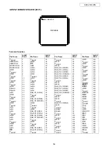
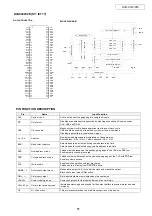
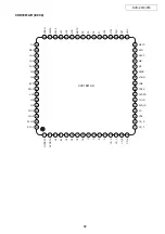
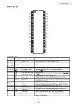
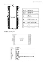
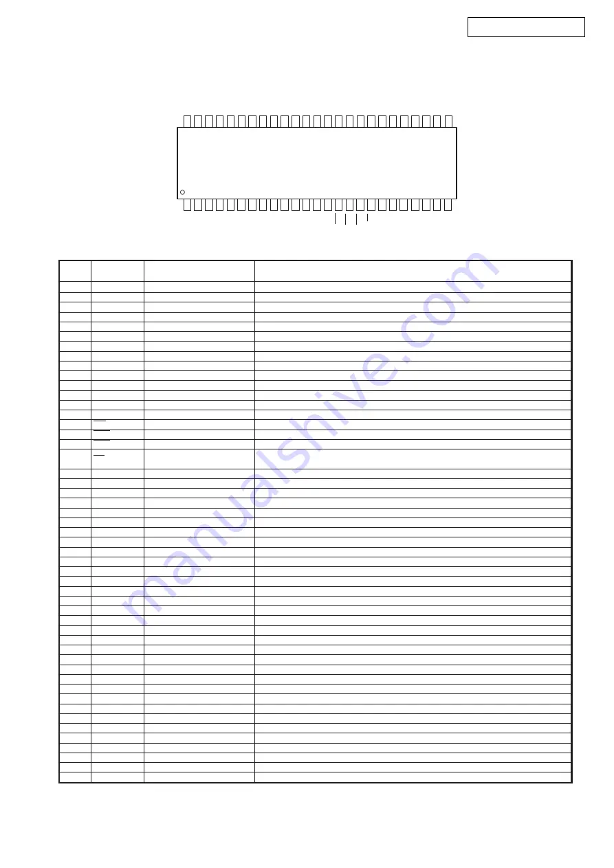
16M SDRAM (MA: IC402)
1
2
3
4
5
6
7
8
9
10
11
12
13
14
15
16
17
18
19
20
21
42
41
40
39
38
37
36
35
34
33
32
31
30
29
28
27
26
25
24
23
22
43
44
45
46
47
48
49
50
A
9
V
DD
DQ
1
DQ
0
DQ
3
DQ
2
DQ
7
DQ
6
DQ
5
DQ
4
A
0
A
1
A
2
A
3
V
DD
V
SSQ
V
SSQ
LDQM
WE
CAS
RAS
CS
BA
A
10
/AP
V
SS
N.C
CKE
CLK
UDQM
N.C/RFU
V
SSQ
DQ
10
DQ
11
V
DDQ
V
SSQ
DQ
14
DQ
15
V
SS
DQ
13
DQ
12
V
DDQ
DQ
9
DQ
8
A
8
A
7
A
6
A
5
A
4
V
DDQ
V
DDQ
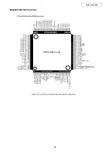
16M SDRAM (TSOP)-8 (DM: IC103, 104)
K4S161622D-TC80
W981616AH-8
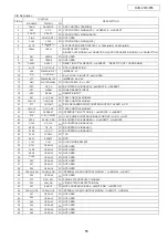
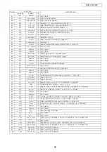
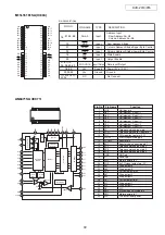
Terminal Function
1
V
DD
Power Supply/Ground
Power and ground for the input buffer and the core logic
2
DQ
0
Data Input/Output
Data input/output are mutiplexed on the same pin
3
DQ
1
Data Input/Output
Data input/output are mutiplexed on the same pin
4
V
SSQ
Data Output Power/Ground
Isolated power supply and ground for the output buffer
5
DQ
2
Data Input/Output
Data input/output are mutiplexed on the same pin
6
DQ
3
Data Input/Output
Data input/output are mutiplexed on the same pin
7
V
DDQ
Data Output Power/Ground
Isolated power supply and ground for the output buffer
8
DQ
4
Data Input/Output
Data input/output are mutiplexed on the same pin
9
DQ
5
Data Input/Output
Data input/output are mutiplexed on the same pin
10
V
SSQ
Data Output Power/Ground
Isolated power supply and ground for the output buffer
11
DQ
6
Data Input/Output
Data input/output are multiplexed on the same pin
12
DQ
7
Data Input/Output
Data input/output are multiplexed on the same pin
13
V
DDQ
Data Output Power/Ground
Isolated power supply and ground for the output buffer
14
L DQM
Data Input/Output Mask
Blocks data input when active
15
WE
Write Enable
Enables write operation and row precharge
16
CAS
Column Address Strobe
Latches column address on the positive going edge of the CLK at low
17
RAS
Row Address Strobe
Latches row address on the positive going edge of the CLK at low
18
CS
Chip Select
Disables or enables device operation by masking or enabling all
inputs except CLK, CKE, and LDQM
19
BA
Bank Select Address
Selects bank to be activated during row address latch time
20
A
10
/AP
Address
Row/column addresses are multiplexed on the same pin
21
A
0
Address
Row/column addresses are multiplexed on the same pin
22
A
1
Address
Row/column addresses are multiplexed on the same pin
23
A
2
Address
Row/column addresses are multiplexed on the same pin
24
A
3
Address
Row/column addresses are multiplexed on the same pin
25
V
DD
Power Supply/Ground
Power and ground for the input buffer and the core logic
26
V
SS
Power Supply/Ground
Power and ground for the input buffer and the core logic
27
A
4
Address
Row/column addresses are multiplexed on the same pin
28
A
5
Address
Row/column addresses are multiplexed on the same pin
29
A
6
Address
Row/column addresses are multiplexed on the same pin
30
A
7
Address
Row/column addresses are multiplexed on the same pin
31
A
8
Address
Row/column addresses are multiplexed on the same pin
32
A
9
Address
Row/column addresses are multiplexed on the same pin
33
N. C
No Connection
No connect pin
34
CKE
Clock Enable
Masks system clock to freeze operation from the next clock cycle
35
CLK
System Clock
Active on the positive going edge to sample all inputs
36
U DQM
Data Input/Output Mask
Blocks data input when active
37
N. C/RFU
NC/Reserved
No connect pin
38
V
DDQ
Data Output Power/Ground
Isolated power supply and ground for the output buffer
39
DQ
8
Data Input/Output
Data input/output are multiplexed on the same pin
40
DQ
9
Data Input/Output
Data input/output are multiplexed on the same pin
41
V
SSQ
Data Output Power/Ground
Isolated power supply and ground for the output buffer
42
DQ
10
Data Input/Output
Data input/output are multiplexed on the same pin
43
DQ
11
Data Input/Output
Data input/output are multiplexed on the same pin
44
V
DDQ
Data Output Power/Ground
Isolated power supply and ground for the output buffer
45
DQ
12
Data Input/Output
Data input/output are multiplexed on the same pin
46
DQ
13
Data Input/Output
Data input/output are multiplexed on the same pin
47
V
SSQ
Data Output Power/Ground
Isolated power supply and ground for the output buffer
48
DQ
14
Data Input/Output
Data input/output are multiplexed on the same pin
49
DQ
15
Data Input/Output
Data input/output are multiplexed on the same pin
50
V
SS
Power Supply/Ground
Power and ground for the input buffer and the core logic
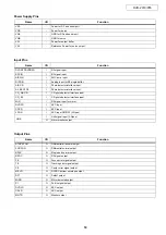
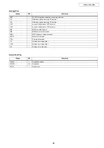
Pin Name
Function
Pin No.
Symbol
Summary of Contents for DVD-2910
Page 29: ...29 DVD 2910 955 BLOCK DIAGRAM ...
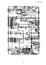
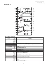
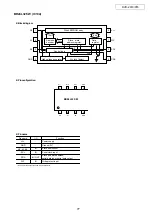
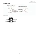
Page 48: ...48 DVD 2910 955 CXD2753R IC602 Pin Assignment Block Diagram ...
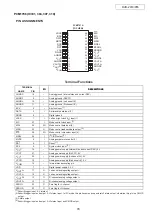
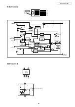
Page 79: ...79 DVD 2910 955 TA76432FC IC902 PC123 IC909 COLLECTOR EMITTER ANODE CATHODE TOP VIEW ...
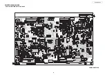
Page 81: ...81 DVD 2910 955 PRINTED WIRING BORDS GU 3612 MAIN PWB P W B UNIT ASS Y COMPONENT SIDE ...
Page 82: ...82 DVD 2910 955 GU 3612 MAIN PWB P W B UNIT ASS Y FOIL SIDE ...
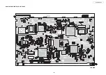
Page 83: ...83 DVD 2910 955 GU 3615 VODEO P W B UNIT ASS Y COMPONENT SIDE ...
Page 84: ...84 DVD 2910 955 GU 3615 VODEO P W B UNIT ASS Y FOIL SIDE ...
Page 85: ...85 DVD 2910 955 GU 3616 AUDIO POWER P W B UNIT ASS Y COMPONENT SIDE ...
Page 86: ...86 DVD 2910 955 GU 3616 AUDIO POWER P W B UNIT ASS Y FOIL SIDE ...
Page 117: ...DVD 2910 955 117 GU 3615 1 VIDEO P W B V6 V7 V8 V1 V2 V3 V4 V5 ...

