background image

G586SP/G586SP AIO

45

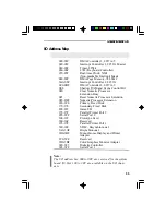
Large Mode

The Large mode is the extended HDD access mode sup-
ported by the G586SP AIO system board. Some IDE  HDDs
have more than 1024 cylinders without LBA support (in
some cases, you may not want the LBA mode). The system
board provides another alternative to support these kinds of
HDD.

The BIOS tells the operating system that the number of
cylinders is 1/2 of actual and that the number of heads is
double the actual. During the disk access, the reverse conver-
sion is done by the INT13h routine.

Example of Large mode:

CYLS.     HEADS     SECTORS     MODE
1120

16

59

NORMAL

 560

32

59

LARGE

Maximum HDD size:

no.Cylinders

(1024)

x no. Heads

( 32)

x no.Sectors

( 63)

x bytes per sector ( 512)

1 Gigabyte

During the HDD accessing, the IDE controller will transform
the logical address described by the sector, head and cylinder
number into its own physical address inside the HDD.

The maximum HDD size supported by the LBA mode is 8.4
Gigabytes. It is obtained by the following formula.

no.Cylinders

(1024)

x no. Heads

( 225)

x no.Sectors

( 63)

x bytes per sector ( 512)

8.4 Gigabyte

Summary of Contents for G586SP

Page 1: ...G586SP G586SPAIO Rev 0 SystemBoard User sManual D29160226 ...

Page 2: ...icular purpose The information in this document is subject to change without notice DFI Inc reserves the right to make revisions to this publication and to make changes to any and or all parts of its content at any time without obligation to notify any person or entity of such changes Further DFI Inc assumes no responsibility for any errors that may appear in this document DFI is a registered trad...

Page 3: ...lar installation If this equipment does cause harmful interference to radio or television reception which can be determined by turning the equipment off and on the user is encouraged to try to correct the interference by one or more of the following measures Reorient or relocate the receiving antenna Increase the separation between the equipment and the receiver Connect the equipment into an outle...

Page 4: ...es 16 JumperSettings 17 CacheConfiguration 21 CPUInstallation 23 InstallationProcedure 24 ClearanceRequirements 26 FanExhaust 26 Built inPorts 27 SerialPorts 27 PS 2MousePort 28 ParallelPort 28 FloppyDiskDriveController 28 ConnectingtheFloppyandHardDiskCable 29 ConnectingtheFloppyDisk 29 ConnectingtheIDEHardDiskInterface 30 AddingaSecondIDEHardDrive 31 PreparinganIDEDriveforUse 31 InstallingExpans...

Page 5: ...tupDefaults 42 PasswordSetting 42 IDEHDDAutoDetection 43 HDDLowLevelFormat 46 Save ExitSetup 47 ExitWithoutSaving 47 System Error Report 48 AppendixA AwardBIOSHardDiskTable 52 AppendixB Memory I OMaps 54 AppendixC PCII OPinAssignments 56 AppendixD ISAI OPinAssignments 57 AppendixE SystemOverview 58 AppendixF ConnectorPinAssignments 61 AppendixG VGAMPEGSupportModeList 72 ...

Page 6: ...troller can display graphic resolutions up to 1024 x 768 256 colors 75Hz at 1MB DRAM and up to 1280x1024 256 colors 60Hz at 2MB DRAM The built in VGA function also supports video playback VESA DDC1 and DDC2B Both the G586SP and G586SP AIO are equipped with three dedicated PCI slots two dedicated ISA slots and one shared PCI ISA slot The board has two bus master PCI IDE con nectors Bus mastering re...

Page 7: ...memory is shared between the CPU and the graphics controller Four 72 pin SIMM sockets 2MB to 256MB onboard memory Uses EDO or fast page mode x32 or x36 DRAM 60 or 70ns Supports 256KB 512KB or 1MB L2 cache direct map WB or WT Uses 32Kx8 64Kx8 or 128Kx8 SRAM Onboard asynchronous SRAM cache Uses Intel COAST compatible Rev 1 2 160 pin cache module slot for optional pipelined burst or synchronous cache...

Page 8: ...1024x768 64K colors 75Hz 1280x1024 256 colors 60Hz TwoBusMasterPCIIDEConnectors PIO Mode 3 4 Enhanced IDE data transfer rate up to 16 6MB sec DMA Mode 2 Bus Master IDE data transfer rate up to 22 2MB sec Bus mastering reduces CPU utilization during disk transfer ATAPI IDE CD ROM supported I O Interface Winbond super I O controller Supports 360KB 720KB 1 2MB and 1 44MB floppy drives Two NS 16C550A ...

Page 9: ...6SP G586SP AIO package contains the following items G586SP G586SP AIO system board G586SP G586SP AIO user s manual One 34 pin floppy disk drive cable One 40 pin hard disk drive cable One 25 pin printer port cable for chassis mounting One card edge bracket with serial port cable One 16 pin cable for the VGA connector One set of IDE software drivers One set of VGA drivers G586SP AIO only Option PS 2...

Page 10: ...tricity direct sunlight excessive humidity extreme cold and water can damage the operational capabilities of your system board Avoid placing the unit on surfaces such as carpeted floors These areas also attract static electricity which can damage some circuits on your system board Make sure the power source has a properly grounded three pronged socket It is essential that the power connection be p...

Page 11: ...ts edges only Be careful not to touch any of the components contacts or connections especially gold contacts on the board 5 Avoid touching the pins or contacts on all modules and connectors Hold modules and connectors by their ends Warning Electrostatic discharge ESD can damage your processor disk drives add in boards and other components Perform the upgrade instruction procedures described at an ...

Page 12: ... the screws holding the original system board and remove the board from the system Save the screws 5 Remove the system board from its original packing box Be careful to avoid touching all connectors and pins on the board Please refer to the handling instructions on page 6 for proper handling techniques 6 Insert the SIMMs into the SIMM banks on the system board The quantity and location of the SIMM...

Page 13: ...G586SP G586SPAIO 13 BoardLayout ...

Page 14: ...ard supports 2MB to 256MB of memory using 72 pin SIMMs Single In line Memory Module with the following two types of memory and sizes 1 Single sided SIMMs 1MB 4MB 16MB and 64MB 2 Double sided SIMMs 2MB 8MB and 32MB The SIM sockets are divided into two banks on the system board Each bank consists of 2 SIMM sockets The board uses x32 or x36 60 0r 70ns SIMMs You will need 2 or 4 pieces of SIM modules ...

Page 15: ...8Mx36 8Mx36 8Mx36 8Mx36 16Mx36 16Mx36 SIMM2 1Mx36 1Mx36 1Mx36 2Mx36 2Mx36 2Mx36 2Mx36 2Mx36 4Mx36 4Mx36 4Mx36 4Mx36 4Mx36 4Mx36 8Mx36 8Mx36 8Mx36 8Mx36 8Mx36 8Mx36 8Mx36 16Mx36 16Mx36 SIMM4 256Kx36 512Kx36 1Mx36 256Kx36 512Kx36 1Mx36 2Mx36 256Kx36 512Kx36 1Mx36 2Mx36 4Mx36 256Kx36 512Kx36 1Mx36 2Mx36 4Mx36 8Mx36 256Kx36 Bank1 SIMM3 256Kx36 512Kx36 1Mx36 256Kx36 512Kx36 1Mx36 2Mx36 256Kx36 512Kx36 ...

Page 16: ...the module aligned with the key on the socket 2 Seat the module at a 45o angle into the bank Make sure it is completely seated Tilt the module upright until it locks in place in the socket MemorySize 132MB 136MB 144MB 160MB 192MB 256MB Bank0 SM3 16Mx36 16Mx36 16Mx36 16Mx36 16Mx36 16Mx36 SM4 16Mx36 16Mx36 16Mx36 16Mx36 16Mx36 16Mx36 SM2 512Kx36 1Mx36 2Mx36 4Mx36 8Mx36 16Mx36 Bank1 SM1 512Kx36 1Mx36...

Page 17: ...O n Off O n Off O n Off O n Off JP8 O n Off O n Off O n Off O n Off O n Frequency Ratio 1 5x 1 5x 1 5x 2x 2x 2 5x 2 5x 3x 3x CPUSpeed 75MHz 90MHz 100MHz 120MHz 133MHz 150MHz 166MHz 180MHz 200MHz JumperJP16 CPUVoltageType Set JP16 pins 1 2 On if the voltage of your CPU is 3 3V Std VR Set JP16 pins 3 4 to On if the voltage of your CPU is 3 45 VRE which is the default setting JumpersJP10andJP11 Onboa...

Page 18: ...ard is installed with asynchronous cache SRAM Set pins 2 3 to On if the system board is installed with burst pipeline burst cache SRAM The default is set to pins 2 3 On If you are install ing a cache module make sure the cache chips have been removed from the SRAM sockets JumperJP18 L1CacheMode Jumper JP18 is used to select the level 1 cache mode Set pins 1 2 to On for write back cache and pins 2 ...

Page 19: ...set JP3 to Off JumperJP5 G586SPAIOonly Onboard VGA Interrupt Set JP5 to On VGA interrupt enabled only when using the VGA feature connector By enabling JP5 you will lose INTA of PCI Slot 1 The default is set to Off disabled JumperJP6 PCIBusClock The default of jumper JP6 is Off CPU Bus Clock 2 If JP6 is set to Off the CPU s external speed will be divided into 2 You can set JP6 to On 32MHz if you ar...

Page 20: ...set your password first power off the computer and set pins 2 3 to On Wait at least one minute and set pins 1 2 to On then turn on your computer The password has now been cleared and the CMOS is back to its default You may enter a new password and or change to a new setting JumperJP13 FlashEPROMType Set JP13 pins 1 2 to On if you are using a 5V Flash EPROM 29F010 29EE010 Set pins 2 3 to On if you ...

Page 21: ...dule 1 Locate the 160 pin cache module slot on the system board Position the cache module above the slot Make sure pin 1 of the cache module is aligned with pin 1 of the slot Carefully slide the module into the slot Press firmly on top of it to seat it properly Note Do not use 5V SRAM as they will not function properly You must first remove the onboard SRAM and or TAG SRAM and select the appropria...

Page 22: ...BIOS Features Setup menu of the Award PnP BIOS CMOS Setup Utility is set to Enabled Note With the cache module installed in the cache module slot the length of the add on card in PCI Slot 4 is limited to 205 mm only if its components protrude more than 5 mm from the components and or solder side of the card ...

Page 23: ... and heat sink may be hot if the system has been running To avoid the possibility of a burn power the system off and let the processor and heat sink cool for 10 minutes The 321 pin ZIF socket consists of five rows of pin holes on each side To prevent improper OverDrive Processor installation the ZIF socket has a Plug Keying mechanism Several holes in the socket are plugged so that OverDrive Proces...

Page 24: ...ack Do not use screwdrivers or other tools to open the socket or you may damage the system or socket It may be necessary to initially apply a small amount of sideways force to free the handle from its retaining tab Once clear of the tab the handle will open relatively easily Installation Procedure 2 Once the lever is completely up remove the old CPU by carefully lifting it straight out of the sock...

Page 25: ...If the CPU will not insert easily verify pin 1 of the CPU is aligned with pin 1 of the socket Applying too much pressure can damage the CPU or the socket 4 Push the handle down until the handle locks into place The top plate will slide forward You will feel some resistance as the pressure starts to secure the CPU in the socket This is normal and will not damage the CPU However if the handle is not...

Page 26: ...r floppy drive hard drive CD ROM etc must be routed clear of the CPU and its airspace FanExhaust The CPU must be kept cool by using a fan exhaust configuration in connection with the heatsink The temperature of the air entering the fan heatsink cannot exceed 45 C 113 F The ambient or room temperature must be below 37 C 99 F for a system installed with the 3 3V Pentium Upgrade Processor In order to...

Page 27: ... system I O addresses 1 COM 1 3F8h 2 COM 2 2F8h Connecting the Serial Ports J4 J5 Two DB 9P serial port cables are provided with the mother board They are mounted on a card edge bracket along with the optional PS 2 mouse cable The upper serial port cable should be used for the COM 1 primary serial port connect it to Connector J4 on the motherboard The lower serial port cable should be used for the...

Page 28: ...ended Capabilities Port standard The parallel port on your system board can be set to any of the following system I O addresses 1 3BC 3BE Hex 2 378 37A Hex Default 3 278 27A Hex Connecting the Parallel Printer Port Attach the DB 25S printer port cable which came with the motherboard to Connector J8 Make sure the colored stripe on the ribbon cable aligns with pin 1 of Connector J8 Use a small nutdr...

Page 29: ...oard The colored edge of the ribbon should be aligned with pin 1 of connector J11 Step2 Install the other 34 pin header connector s into the disk drive s with the colored edge of the daisy chained ribbon cable aligned with pin 1 of the drive edge connector s The end most connector should be attached to the drive you want to designate as Drive A Pin 1 Stripe Floppy Drive Connector J11 J12 Primary I...

Page 30: ...ecting two hard drives install the 40 pin connector of the IDE cable into the primary IDE shrouded header Connector J12 If you are adding a third or fourth IDE device install the 40 pin connector of the other IDE cable into the secondary IDE shrouded header Connector J13 Step2 Install the other 40 pin header connector s into the device with the colored edge of the ribbon cable aligned with pin 1 o...

Page 31: ...rent manufacturers will not function properly when used together The problem lies in the hard drives not the system board Preparing an IDE Drive for Use IDE disk drives are already low level formatted with any bad track errors entered when shipped by the drive manufac turer Do not attempt to do a low level format or you may cause serious damage to the drive To use an IDE drive you need to enter th...

Page 32: ...ted to 205mm measured from the bracket of the card The length of the add in card in PCI slot 4 is limited to 205mm only if its components protrude more than 5mm from the components and or solder side of the card The locations of the expansion slots are shown on page 8 Note The BIOS needs to be configured for the PCI add on cards installed in the PCI slots Refer to the PCI Configuration Setup chapt...

Page 33: ... doubt refer to the Board Configura tion section 2 Verify that all SIMMs are seated securely into the bank sockets 3 Make sure the SIMMs are in the correct locations 4 Check that all populated memory banks are filled with correctly sized SIMMs 5 If your board fails to function place the board on a flat surface and seat all socketed components gently press each component into the socket 6 If you ma...

Page 34: ...trl Alt and Del keys at the same time If you do not press these keys at the correct time and the system does not boot the following error message will appear Press Del to enter Setup If you have set a password and selected System in the Security Option of the BIOS Feature Setup menu you will be prompted for the password everytime the system is rebooted or any time you try to enter Setup Type in th...

Page 35: ...ect Item Change Color Shift F2 Tue Nov 7 1995 11 42 28 MODE LBA AUTO AUTO AUTO SIZE 0 0 0 0 1 44M 3 5 in 1 2M 5 25 in EGA VGA All Errors Use the arrow keys to highlight the option you want and press Enter StandardCMOSSetup Use the arrow keys to highlight Standard CMOS Setup and press Enter a screen similar to the one on the next page will appear STANDARD CMOS SETUP BIOSFEATURES SETUP CHIPSET FEATU...

Page 36: ... for a hard disk drive larger than 528 megabytes If you decide not to accept the LBA mode you can either specify your selection in the IDE HDD Auto Detection menu or use the User option described below User This type is user definable and allows you to enter the specifications yourself directly from the keyboard Six categories of information are required Size Cylinders Heads Precomp LandZone and S...

Page 37: ... is used to select the type of video adapter installed in your system Halton This category controls whether the system will halt in case an error is detected during power up No Errors The system boot will not stop for any detected errors All Errors The system will stop whenever the BIOS detects a nonfatal error All But Keyboard The system will stop for any error except a keyboard error All But Dis...

Page 38: ...a screen similar to the one below will appear ROM PCI ISABIOS 2A5IDD49 BIOS FEATURES SETUP AWARD SOFTWARE INC Virus Warning CPU Internal Cache External Cache Quick Power On Self Test Boot Sequence Swap Floppy Drive Boot Up Floppy Seek Boot Up NumLock StatuS Boot Up System Speed Gate A20 Option Memory Parity Check Typematic Rate Setting Typematic Rate Chars Sec Typematic Delay Msec Security Option ...

Page 39: ... 55 The Virus Warning option may be set to Enabled or Disabled When enabled the BIOS issues a warning when any program or virus sends a Disk Format command or attempts to write to the boot sector of the hard disk drive If you are installing or running certain operating systems such as Windows 95 please disable the Virus Warning or the operating system may not install nor work If you choose System ...

Page 40: ...he highlight bar to the option you wish to change or modify Use the Page Up Page Down or keys to make the corresponding changes If the changes you made are incorrect or you change your mind press F6 or F7 to return to the default settings Press Esc after making the changes to return to the main menu PowerManagementSetup Use the arrow keys to highlight Power Management Setup and press Enter A scree...

Page 41: ...IOS 2A5IDD49 PCI ONBOARD I O SETUP AWARD SOFTWARE INC PnPBIOS Auto Config 1st Available IRQ 2nd Available IRQ 3rd Available IRQ 4th Available IRQ PCI IRQ Activated By PCI IDE IRQMap To Primary IDE INT Secondary IDE INT CPU PCI Post Write Rate Latency for CPU PCI CPU PCI Burst Mem Write CPU PCI Post Mem Write Internal PCI IDE IDE Primary Mater PIO IDE Primary Slave PIO IDE Secondary Master PIO IDE ...

Page 42: ...l be loaded LoadSetupDefaults The Load Setup Defaults option loads optimized settings from the BIOS ROM Use the Setup default values as stan dard values for your system Highlight this option on the main menu and press Enter The message below will appear Load Setup Defaults Y N N Type Y and press Enter to load the Setup default values PasswordSetting If you want to set a password make sure that the...

Page 43: ...press Enter instead of typing in a new password Press the Esc key to return to the main menu IDEHDDAutoDetection This option detects the hard disk parameters for the hard disk drives installed in your system Highlight this option and press Enter A screen similar to the one on the next page will appear ROM PCI ISA BIOS 2A5IDD49 CMOS SETUP UTILITY A WARD SOFTWARE INC CYLS HEADS PRECOMP LANDZ SECTOR ...

Page 44: ...ccess mode in which neither the BIOS nor the IDE controller will make any transformations during hard drive access The maximum number of cylinders heads and sectors for Normal mode are 1024 16 and 63 respectively no Cylinders 1024 x no Heads 16 x no Sectors 63 x bytes per sector 512 528 Megabyte If you set your HDD to Normal mode the maximum acces sible HDD size will be 528 Megabytes even though i...

Page 45: ...he actual During the disk access the reverse conver sion is done by the INT13h routine Example of Large mode CYLS HEADS SECTORS MODE 1120 16 59 NORMAL 560 32 59 LARGE Maximum HDD size no Cylinders 1024 x no Heads 32 x no Sectors 63 x bytes per sector 512 1 Gigabyte During the HDD accessing the IDE controller will transform the logical address described by the sector head and cylinder number into i...

Page 46: ...he arrow keys to select an option and press Enter to accept the option Press Esc when done HDDLowLevelFormat This option will format set the interleave mode and do a media analysis of your hard drives Highlight this option and press Enter A screen similar to the one below will appear Hard Disk Low Level Format Utility SELECT DRIVE BAD TRACK LIST PREFORMAT Current select drive is C DRIVE C CYLINDER...

Page 47: ...ill once again see the initial diagnostics on the screen If you wish to make additional changes to the setup press Ctrl Alt Esc simultaneously or Del after memory testing is done ExitWithoutSaving When you do not want to save the changes you have made highlight this option and press Enter The message below will appear Quit Without Saving Y N N Type Y and press Enter The system will reboot and you ...

Page 48: ...eeps ErrorMessages One or more of the following messages may be displayed if the BIOS detects an error during the POST DISK BOOT FAILURE INSERT SYSTEM DISK AND PRESS ENTER No boot device was found Insert a system disk into Drive A and press Enter If the system normally boots from the hard drive make sure the controller is inserted correctly and all cables are properly attached Also be sure the dis...

Page 49: ... HARD DISK CONTROLLER Cannot initialize controller Make sure the card is correctly and firmly installed in the bus Be sure the correct hard drive type is selected in Setup Also check to see if any jumper needs to be set correctly on the hard drive FLOPPY DISK CNTRLR ERROR OR NO CNTRLR PRESENT Cannot find or initialize the floppy drive controller Make sure the controller is installed correctly and ...

Page 50: ...ic location You can use this location along with the memory map for your system to find and replace the bad memory chips MEMORY PARITY ERROR AT Indicates a memory parity error at a specific location You can use this location along with the memory map for your system to find and replace the bad memory chips OFFENDING SEGMENT This message is used in conjunction with the I O CHANNEL CHECK and RAM PAR...

Page 51: ...R SEGMENT Indicates a parity error in Random Access Memory SYSTEM HALTED CTRL ALT DEL TO REBOOT Indicates the present boot attempt has been aborted and the system must be rebooted Press and hold down the CTRL and ALT keys and press DEL simultaneously ...

Page 52: ...977 1024 1224 1224 1224 1024 4 4 6 8 6 4 8 5 15 3 5 7 8 7 4 5 7 7 5 7 5 4 5 9 7 11 15 Example Model Write Precomp 128 300 300 512 512 None 256 None None None None None 128 None 0 300 None 512 300 300 300 0 None None None None None Land Zone 305 615 615 940 940 615 511 733 901 820 855 855 319 733 663 977 977 1023 732 732 733 336 976 1023 1223 1223 1223 Reserved TEAC SD510 MMI 112 5412 Seagate ST225...

Page 53: ...776 684 8 11 11 9 10 12 13 14 2 16 15 6 5 5 6 6 8 16 Example Model Write Precomp None None None None None None None None None None None None None None None None None None Land Zone 1023 1023 1023 926 1023 1023 1023 1023 1023 1023 1023 820 1023 1023 852 852 775 685 User Defined Maxtor 1085 Micropolis 1325 Maxtor 1105 1120 4780 Maxtor 1170 CDC 9415 Maxtor 1140 4380 Seagate ST251 Seagate 4053 Miniscr...

Page 54: ...d Memory 009FFFF Board RAM 00A0000 to 128KB Video Reserved for Graphics 00BFFFF Display Memory Display Memory 00C0000 to 160KB I O Reserved for ROM on 00E7FFF Expansion ROM I O Adapter Card 00E8000 to 96KB ROM on System Board BIOS 00FFFFF the System Board 0100000 to Maximum System Board Memory 3FFFFFF Memory 128MB ...

Page 55: ...nsion Busy 0F1 Reset Numeric Processor Extension 0F8 OFF Numeric Processor Extension 1F0 1F8 Primary Fixed Disk 170 178 Secondary Fixed Disk 200 207 Game I O 278 27F Parallel Printer Port 2 2F8 2FF Serial Port 2 300 31F Prototype Card 360 36F Reserved 378 37F Parallel Printer Port 1 380 38F SDLC Bisynchronous 2 3A0 3AF Bisynchronous 1 3B0 3BF Monochrome Display and Printer Adapter 3C0 3CF Reserved...

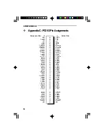
Page 56: ...4 IDSEL 3 3V AD 22 AD 20 Ground AD 18 AD 16 3 3V FRAME Ground TRDY Ground STOP 3 3V SDONE SBO Ground PAR AD 15 3 3V AD 13 AD 11 Ground AD 09 C BE 0 3 3V AD 06 AD 04 Ground AD 02 AD 00 5V I O REQ64 5V 5V B 12V TCK Ground TDO 5V 5V INTB INTD PRSNT1 Reserved PRSNT2 Ground Ground Reserved Ground CLK Ground REQ 5V I O AD 31 AD 29 Ground AD 27 AD 25 3 3V C BE 3 AD 23 Ground AD 21 AD 19 3 3V AD 17 C BE 2...

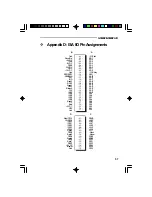
Page 57: ...12 13 14 15 16 17 18 C SBHE LA23 LA22 LA21 LA20 LA19 LA18 LA17 Memr Memw SD08 SD09 SD10 SD11 SD12 SD13 SD14 SD15 v AppendixD ISAI OPinAssignments A I OChck SD7 SD6 SD5 SD4 SD3 SD2 SD1 SD0 I OChrdy AEN SA19 SA18 SA17 SA16 SA15 SA14 SA13 SA12 SA11 SA10 SA9 SA8 SA7 SA6 SA5 SA4 SA3 SA2 SA1 SA0 B Gnd ResetDrv 5VDC IRQ9 5VDC DRQ2 12VDC O W S 12VDC Gnd SEMEMW SEMEMR IOW IOR Dack3 DRQ3 Dack1 DRQ1 Refresh ...

Page 58: ...h6 ReservedforUser Ch7 ReservedforUser Note DMA controller 1 supports 8 bit data transfer DMA controller 2 supports 16 bit data transfer AddressGenerationforDMAChannels3to0 Source DMAPageMemory DMAController1 Address A23 A16 A15 A0 AddressGenerationforDMAChannels7to5 Source DMAPageMemory DMAController2 Address A23 A17 A16 A1 v AppendixE SystemOverview DMAChannels ...

Page 59: ...from INTR2 IRQ3 Serial Port 2 IRQ4 Serial Port 1 IRQ5 Parallel Port 2 or 3 IRQ6 Diskette Controller IRQ7 Parallel Port 1 or 2 The one on board parallel port can be configured to either Paral lel Port 1 2 or 3 Parallel Port 1 uses I O address 3BCh Parallel Port 2 I O address 378h and Parallel Port 3 uses I O address 278H IRQ8 RealtimeClockINT IRQ9 Software Redirected toINT0AH IRQ2 IRQ10 Reserved IR...

Page 60: ... IRQ6 IRQ7 SystemTimers Channel0 SystemTimer IRQ0 Channel1 RefreshRequestGenerator 15us Rate Generator Period Signal Tone Generation for Speaker Channel2 Real TimeClock Address 00 01 02 03 04 05 06 07 08 09 0 A 0 B 0 C 0 D Function Seconds SecondAlarm Minutes MinuteAlarm Hours HourAlarm DayofWeek DateofMonth Month Year RegisterA RegisterB RegisterC RegisterD ...

Page 61: ...Data Reserved Ground 5V KeyboardClock Reserved Pin 1 2 3 4 5 6 Function MouseData Reserved Ground 5V MouseClock Reserved ConnectorJ2 PS 2KeyboardConnector Pin 1 2 3 4 5 Function KeyboardClock KeyboardClock NotConnected Ground 5V ConnectorJ3 PS 2MouseConnector ConnectorJ2 ATKeyboardConnector ...

Page 62: ...ial Ports Pin 1 2 3 4 5 6 7 8 9 Function DCD Data Carrier Detect RX ReceiveData TX TransmitData DTR DataTerminalReady Ground Signal Ground DSR DataSetReady RTS RequesttoSend CTS Clear to Send RI Ring Indicator ConnectorJ6 12VFanConnector Pin 1 2 Function 12V Ground ...

Page 63: ...Connector Pin 1 2 3 4 5 6 7 8 9 10 11 12 13 14 15 16 Function Red Green Blue Monitor ID bit 2 Not Used Ground Red Return ground Green Return ground Blue Return ground Key Sync Return ground Notused DDCDA T Horizontal Sync Vertical Sync DDCCCK Notused ...

Page 64: ... 12 13 14 15 16 17 18 19 20 21 22 23 24 25 Function Strobe Data0 Data1 Data2 Data3 Data4 Data5 Data6 Data7 Ack Busy PaperEmpty Select Autofd Error Init Slctin Ground Ground Ground Ground Ground Ground Ground Ground ConnectorJ8 Parallel Printer Port ...

Page 65: ...G586SP G586SPAIO 65 ConnectorJ9 PowerConnector Pin 1 2 3 4 5 6 7 8 9 10 11 12 Function PowerGood 5V 12V 12V Ground Ground Ground Ground 5V 5V 5V 5V ...

Page 66: ...13 14 15 16 17 18 19 20 21 22 23 24 25 26 Connector J10 G586SPAIO FeatureConnector Function PD0 PD1 PD2 PD3 PD4 PD5 PD6 PD7 Enpclk EBlank EHSync EVSync Ground Ground Ground Ground EnVideo EnSync EnPclk Notused Ground Ground Ground Ground Notused Ground ...

Page 67: ... 17 18 19 20 21 22 23 24 25 26 27 28 29 30 31 32 33 34 Function Ground DENSEL Ground Reserved Ground Drate0 Ground Index Ground MTR0 Ground DR1 Ground DR0 Ground MTR1 Drate1 Dir Ground Step Ground WriteData Ground WriteGate Ground Track0 MSEN WrProtect Ground ReadData Ground HeadSelect Ground DiskChange ...

Page 68: ...D 2 D13 D 1 D14 D 0 D15 Ground Reserved Reserved Ground IOW Ground IOR Ground Reserved BALE Reserved Ground IRQ IOCS16 SA1 Pin 1 2 3 4 5 6 7 8 9 10 11 12 13 14 15 16 17 18 19 20 21 22 23 24 25 26 27 28 29 30 31 32 33 ConnectorJ12andJ13 Primary Secondary IDE Hard Disk Drive Connectors ...

Page 69: ...G586SP G586SPAIO 69 Pin 1 2 3 4 Function 3 6V Lithium Battery Key GND GND ConnectorJ14 External Battery Pin 34 35 36 37 38 39 40 Function Reserved SA0 SA2 HCS0 HCS1 LED Ground ...

Page 70: ...0 ConnectorJ17 IDELED Pin 1 2 Function Signal LEDPower ConnectorJ18 SuspendSwitch Pin 1 2 Function Signal GND ConnectorJ19 GreenLED Pin 1 2 Function Signal LEDPower Pin 1 2 Function Signal LEDPower ConnectorJ20 TurboLED ...

Page 71: ...n 1 2 Function GND Signal ConnectorJ22 Reset Switch Pin 1 2 Function Ground Reset Pin 1 2 3 4 Function Signal Reserved Ground 5V ConnectorJ24 PowerLED Keylock Pin 1 2 3 4 5 Function LEDSignal Reserved Ground Leylock Signal Ground ConnectorJ23 Speaker ...

Page 72: ... ü 8 0 0 X 6 0 0 2 5 6 7 2 1 M B ü ü 8 0 0 X 6 0 0 2 5 6 7 5 1 M B ü ü 8 0 0 X 6 0 0 3 2 K 5 6 1 M B ü 8 0 0 X 6 0 0 3 2 K 6 0 1 M B ü 8 0 0 X 6 0 0 6 4 K 5 6 1 M B ü 8 0 0 X 6 0 0 6 4 K 6 0 1 M B ü 1 0 2 4 X 7 6 8 1 6 6 0 1 M B 1 0 2 4 X 7 6 8 1 6 7 0 1 M B 1 0 2 4 X 7 6 8 1 6 7 5 1 M B 1 0 2 4 X 7 6 8 1 6 8 7 I 1 M B 1 0 2 4 X 7 6 8 2 5 6 6 0 1 M B ü 1 0 2 4 X 7 6 8 2 5 6 7 0 1 M B ü 1 0 2 4 X 7...

Page 73: ... 6 0 0 6 4 K 7 5 2 M B ü ü 8 0 0 X 6 0 0 1 6 7 M 5 6 2 M B ü ü ü 8 0 0 X 6 0 0 1 6 7 M 6 0 2 M B ü ü 8 0 0 X 6 0 0 1 6 7 M 7 2 2 M B ü ü 8 0 0 X 6 0 0 1 6 7 M 7 5 2 M B ü ü 1 0 2 4 X 7 6 8 1 6 6 0 2 M B 1 0 2 4 X 7 6 8 1 6 7 0 2 M B 1 0 2 4 X 7 6 8 1 6 7 5 2 M B 1 0 2 4 X 7 6 8 1 6 8 7 I 2 M B 1 0 2 4 X 7 6 8 2 5 6 6 0 2 M B ü ü ü 1 0 2 4 X 7 6 8 2 5 6 7 0 2 M B ü ü 1 0 2 4 X 7 6 8 2 5 6 7 5 2 M B...

Reviews: