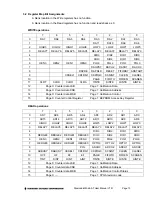
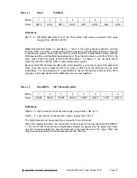
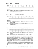
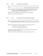
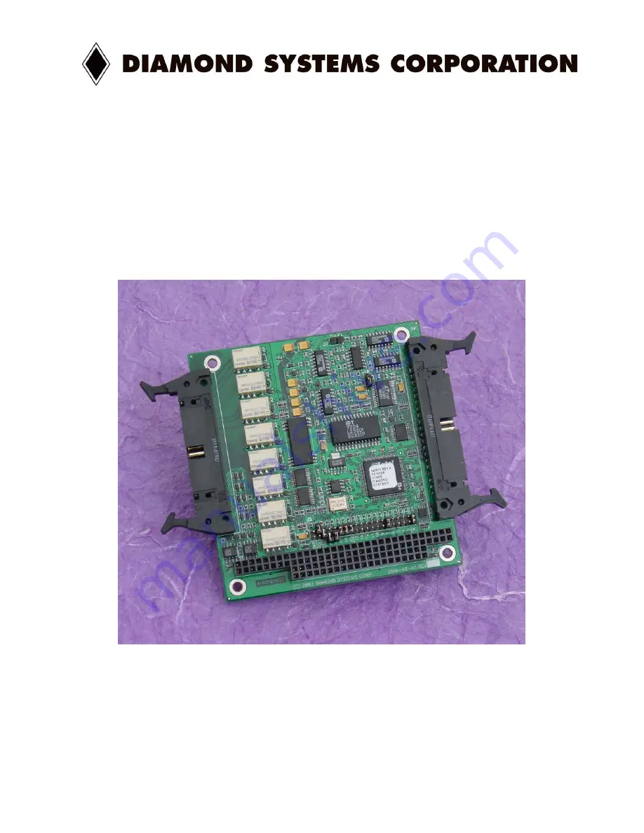
background image


250 


DIAMOND-MM-48-AT 

Autocalibrating 16-bit Analog I/O PC/104 Module 

With Relays and Optocouplers


User Manual V1.01 


 Copyright 2004 

Diamond Systems Corporation 

8430-D Central Ave. 

Newark, CA 94560 

Tel (510) 456-7800 

www.diamondsystems.com 

Summary of Contents for DIAMOND-MM-48-AT MM-48-AT

Page 1: ...8 AT Autocalibrating 16 bit Analog I O PC 104 Module With Relays and Optocouplers User Manual V1 01 Copyright 2004 Diamond Systems Corporation 8430 D Central Ave Newark CA 94560 Tel 510 456 7800 www diamondsystems com ...

Page 2: ...5 I O MAP 9 6 REGISTER DEFINITIONS 11 7 ANALOG INPUT RANGES AND RESOLUTION 27 8 PERFORMING AN A D CONVERSION 28 9 A D SCAN FIFO AND INTERRUPT OPERATION 31 10 ANALOG OUTPUT OVERVIEW 34 11 GENERATING AN ANALOG OUTPUT 35 12 AUTOCALIBRATION OPERATION 36 13 DIGITAL I O OPERATION 37 14 OPTOCOUPLER OPERATION 38 15 RELAY OPERATION 40 16 COUNTER TIMER OPERATION 41 17 SPECIFICATIONS 44 ...

Page 3: ...nput range optional 2048 sample FIFO for reliable high speed sampling Autocalibrated input circuit Analog Outputs 8 analog outputs 12 bit D A resolution 0 4 096V output range 1mV per LSB Autocalibrated output circuit Digital I O 4 programmable direction digital I O lines Edge detection capability with interrupt on change of state Optocoupler Inputs 4 optocoupler inputs 3 28VDC input range Configur...

Page 4: ...e descriptions J1 PC 104 8 bit bus connector J2 PC 104 16 bit bus connector J3 Analog and digital I O connector J4 Relay and optocoupler I O connector J6 Configuration jumper block J7 Factory use only used in factory calibration process J10 5 input range selection bipolar model only ...

Page 5: ... 1 Vout 2 21 22 Vout 3 Vout 4 23 24 Vout 5 Vout 6 25 26 Vout 7 D A Gnd 27 28 Dgnd Extclk 29 30 Gate 0 Out 0 31 32 Clk 1 Gate 1 33 34 Out 1 DIO 0 35 36 DIO 1 DIO 2 37 38 DIO 3 5V 39 40 Dgnd Signal Name Definition Vin 0 15 Analog input channels 0 to 15 all inputs are single ended Vout 0 7 Analog output channels 0 7 DIO 0 3 Digital I O port TTL CMOS compatible programmable direction Extclk External A...

Page 6: ...mmon contact this contact is always used with relay output connections Relay N NC Relay output normally connected contact this contact is connected to the Out N C contact when power is off or when a 0 is written to the relay s control bit in the relay control register and it is disconnected when power is on and a 1 is written to the relay s control bit Relay N NO Relay output normally open contact...

Page 7: ...00 768 Default In Out Out In In In 340 832 In Out Out In Out In 380 896 In Out Out Out In In 3C0 960 In Out Out Out Out In 4 2 Interrupt Level Selection In addition to the base address described above J6 is used to configure hardware interrupt activity Interrupts are used for several functions They can be used to transfer A D data from the board to memory at a rate higher than can be achieved thro...

Page 8: ... back as a 1 For inverted polarity an open circuit low voltage reads as 1 and a high voltage reads as 0 For direct polarity the POL jumper should be absent For inverted polarity install a jumper in the POL location 4 4 Reserved The EWP position on J6 is reserved for a future option and currently has no function 4 5 Analog Input Range On the standard bipolar input range model the input range can be...

Page 9: ...gital I O configuration Digital I O config status readback 5 Digital I O output data Digital I O input and edge data 6 Optocoupler configuration Optocoupler configuration readback 7 D A channel and update control Optocoupler input and edge data 8 Command register Status register 9 Configuration register Configuration register readback 10 FIFO control register FIFO status register 11 Interrupt cont...

Page 10: ...e 0 Counter data CSB Page 1 Calibration Address 14 Page 0 Counter data MSB Page 1 Calibration Control 15 Page 0 Counter Control Register Page 1 EEPROM Access Key Register READ operations 7 6 5 4 3 2 1 0 0 AD7 AD6 AD5 AD4 AD3 AD2 AD1 AD0 1 AD15 AD14 AD13 AD12 AD11 AD10 AD9 AD8 2 HIGH3 HIGH2 HIGH1 HIGH0 LOW3 LOW2 LOW1 LOW0 3 RELAY7 RELAY6 RELAY5 RELAY4 RELAY3 RELAY2 RELAY1 RELAY0 4 DIR3 DIR2 DIR1 DI...

Page 11: ...is an unsigned 12 bit number ranging from 0 to 4095 Base 0 Read A D LSB Bit No 7 6 5 4 3 2 1 0 Name AD7 AD6 AD5 AD4 AD3 AD2 AD1 AD0 Definitions AD7 0 A D LSB data bits 7 0 of the 16 bit value A D data is a signed 16 bit value ranging from 32768 to 32767 Base 1 Write DAC 0 3 MSB Bit No 7 6 5 4 3 2 1 0 Name DA11 DA10 DA9 DA8 Definitions DA11 8 D A data bits 11 8 for the selected channel DA11 is the ...

Page 12: ...the FIFO decrements after each read operation you cannot read out the same A D value more than once unless the FIFO is empty in which case the last byte may be read indefinitely It is the programmer s responsibility to ensure that data is read out of the FIFO properly so that appropriate LSB MSB pairs are read out together Base 2 Read Write A D Channel Register Bit No 7 6 5 4 3 2 1 0 Name HIGH3 HI...

Page 13: ...is register On power up or reset the output register is cleared to all zeroes and all relays reset to their off condition C connected to NC by resetting all RELAY pins to 1 Relays are in the off condition when power is off and remain in that condition when power is applied until a 1 is written to their corresponding control register bit Base 4 Read Write Digital I O Configuration Register Bit No 7...

Page 14: ...ed 1 enabled POL3 0 Select active edge polarity for selected digital input line 0 falling 1 rising An interrupt request will occur when OINTE 1 and a digital input line enabled with OENn exhibits an edge whose polarity matches POLn a qualifying edge If an interrupt request occurs and an additional qualifying edge occurs before the digital interrupt flip flop is reset no additional interrupt reques...

Page 15: ...have as described below DACH2 0 D A channel number valid range 0 7 Base 7 Read Optocoupler Input Port and Edge Detection Register Bit No 7 6 5 4 3 2 1 0 Name OEDGE3 OEDGE2 OEDGE1 OEDGE0 OPTO3 OPTO2 OPTO1 OPTO0 OEDGE3 0 Indicates whether an edge has occurred on the indicated digital input line 1 edge has occurred since last flip flop reset 0 edge has not occurred since last flip flop reset These bi...

Page 16: ...ponds to 0V for the selected D A mode For example for D A in unipolar mode the preset value would be 0 and for D A in bipolar mode the preset value would be 2048 DAPRLD The D A preset register is loaded with the value contained in registers 0 1 After the preset value is loaded into the D A a DAPRE command will update all 8 D A channels with this value RESET Reset the board to a known condition All...

Page 17: ... setting the value indicates the value of an open circuit 1 Open circuit reads as 1 high input reads as 0 0 Open circuit reads as 0 high input reads as 1 ADCH3 0 Current A D channel this is the channel currently selected on board and is the channel that will be used for the next A D conversion unless a new value is written to the channel register before then ...

Page 18: ...lect for counter timer 0 1 1MHz 0 10MHz SCNINT Scan interval This is the time between A D samples during an A D scan An A D scan occurs when SCANEN 1 Base 10 bit 4 and an A D conversion is triggered 1 5 0µS 0 9 3µS CLKEN Enable hardware A D clock 1 Enable hardware A D trigger source is selected with CLKSEL bit software triggers are disabled 0 Disable hardware trigger A D is triggered by setting th...

Page 19: ...tor J3 0 On board clock frequency selected by CKFRQ1 below CKFRQ1 Clock frequency select for counter timer 1 when CKSEL1 0 1 100KHz 0 10MHz CKFRQ0 Clock frequency select for counter timer 0 1 1MHz 0 10MHz SCNINT Scan interval This is the time between A D samples during an A D scan An A D scan occurs when SCANEN 1 Base 10 bit 4 and an A D conversion is triggered 1 5 0µS 1 9 3µS CLKEN Enable hardwar...

Page 20: ...scan that causes the FIFO to reach or exceed its half full point 256 samples 0 Scan mode disabled the ADBUSY bit will remain high for a single conversion Base 10 Read FIFO Status Register Bit No 7 6 5 4 3 2 1 0 Name OVF HF 8F EF PAGE FIFOTH FIFOEN SCANEN OVF FIFO overflow flag 0 no overflow 1 overflow Overflow is defined as the state when the FIFO is full and another A D conversion occurs before a...

Page 21: ... circuit and leaves alone all other bits in this register Writing a 0 to a CLRx bit has no effect on that circuit Each circuit s interrupt flip flop can be reset individually When all interrupt circuits have been reset either by clearing them individually or by disabling them with xINTE 0 the board s interrupt request line will be tristated TINTE Timer interrupt enable 1 Enable interrupts on falli...

Page 22: ...terrupt not pending OINT Optocoupler input interrupt request status 1 One or more qualifying edges have occurred on the optocouplers 0 No qualifying edges have occurred AINT Analog input interrupt request status 1 Interrupt request is pending from A D circuit 0 No interrupt is pending from A D circuit TINTE Readback of TINTE bit described on previous page DINTE Readback of DINTE bit described on p...

Page 23: ...egister an internal load register is loaded Upon issuing a Load command through Base 15 the selected counter s associated register will be loaded with this value For counter 0 it is the middle byte For counter 1 it is the MSB When reading from this register the associated byte of the most recent Latch command will be returned The value returned is NOT the value written to this register Base 14 Rea...

Page 24: ...ignal is high counting is enabled If the GATEn signal is low counting is disabled CTDIS Disable counting on the selected counter The counter will ignore input pulses CTEN Enable counting on the selected counter The counter will decrement on each input pulse LOAD Load the selected counter with the data written to Base 12 through Base 14 or Base 12 and Base 13 depending on which counter is being loa...

Page 25: ...is register will be written to the selected device During EEPROM read operations this register contains the data to be read from the EEPROM and is valid after EEBUSY 0 Page 1 Base 14 The TrimDAC data cannot be read back Base 13 Read Write EEPROM TrimDAC Address Register Bit No 7 6 5 4 3 2 1 0 Name A7 A6 A5 A4 A3 A2 A1 A0 A7 A0 EEPROM TrimDAC address The EEPROM recognizes address 0 127 using addres...

Page 26: ... value of analog output 0 1 enable cal mux and disable user analog input channels 0 disable cal mux enable user inputs TDACEN TrimDAC Enable Writing 1 to this bit will initiate a transfer to the TrimDAC used in the autocalibration process Base 14 Read Calibration Status Register Bit No 7 6 5 4 3 2 1 0 Name 0 TDBUSY EEBUSY CMUXEN TDACEN 0 0 0 TDBUSY TrimDAC busy indicator 0 User may access TrimDAC ...

Page 27: ...alog ground on the board This means that the input voltage will be measured with respect to the board s analog ground A differential input is a three wire input input input and ground and the board will measure the difference between the voltages of the two inputs Diamond MM 48 AT works only with single ended inputs In some cases a differential input can be simulated by connecting the high and low...

Page 28: ... read channels 0 through 15 write 0xF0 to Base 2 Note When you perform an A D conversion the current channel is automatically incremented to the next channel in the selected range Therefore to perform A D conversions on a group of consecutively numbered channels you do not need to write the input channel prior to each conversion For example to read from channels 0 2 write Hex 20 to base 2 The firs...

Page 29: ...ad back as bit 7 in the status register at Base 9 When the A D converter is busy performing an A D conversion this bit is 1 and when the A D converter is idle conversion is done and data is available this bit is 0 Here is a pseudocode explanation Status read base 9 AND 128 or Status read base 9 AND 80 Hex If Status 0 then conversion is complete else A D converter is busy Keep repeating this proced...

Page 30: ...age Example Input range is 10V and A D value is 17761 Input voltage 17761 32768 10V 5 420V For a bipolar input range 1 LSB 1 32768 Full scale voltage For the 10V range 1 LSB 305µV and for the 5V range 1 LSB 153µV Here is an illustration of the relationship between A D code and input voltage for a bipolar input range VFS Full scale input voltage 10V or 5V A D Code Input voltage symbolic formula Inp...

Page 31: ...les and then the interrupt request will occur The basic sequence is as follows 1 A D trigger command occurs 2 A D conversion or A D scan occurs 3 A D data is stored in the FIFO 4 Interrupt request occurs 5 Interrupt routine extracts data from the FIFO and resets the interrup request A D Trigger The A D trigger may come from one of three sources as determined by the control bits CLKEN and CLKSEL CL...

Page 32: ...the expected performance of the application software s interrupt routine including Diamond Systems Universal Driver software Note that in all cases A D data is stored in and read from the FIFO regardless of the FIFOEN setting FIFOEN only controls whether the FIFO flags are used to drive interrupt requests FIFOEN FIFOTH SCANEN Interrupt Operation 0 0 0 Interrupt occurs at the end of each individual...

Page 33: ...d by write to B 0 All channels between LOW and HIGH will be sampled STS stays high during the entire scan multiple A D conversions No interrupt occurs The user program monitors STS and reads all A D values when it goes low 0 1 0 Same operation as case 000 above 0 1 1 Same operation as case 001 above 1 0 0 Single A D conversions are triggered by the source selected with CLKSEL STS stays high during...

Page 34: ...SB or 1 least significant bit The value of this LSB is calculated based on the output range of the circuit On the Diamond MM 48 AT the output range is fixed at 0 4 096V making the formula simple 1 D A LSB 4 096V 4096 1mV 10 3 D A Conversion Formulas and Tables The formulas below explain how to convert between D A codes and output voltages Conversion Formulas for Unipolar Output Ranges Output volta...

Page 35: ...it number The maximum output value is 4095 Therefore the maximum possible output voltage is 4 095V 1mV less than the full scale voltage of 4 096V 11 2 Write the value to the selected output channel First use the following formulas to compute the LSB and MSB values LSB D A Code AND 255 keep only the low 8 bits MSB int D A code 256 strip off low 8 bits keep 4 high bits Example Output code 1776 LSB 1...

Page 36: ...ration multiplexor The offsets of the other DACs relative to DAC 0 are measured at the factory and stored in the EEPROM During calibration the average offset is added to the measured output of DAC 0 and this value is used as the comparison value to minimize overall errors 12 4 Universal Driver Software Support Calibration is simple when using the Diamond Systems Universal Driver software Several f...

Page 37: ...TE bit in Base 11 When DINTE 1 any change of state on any input line will generate an interrupt and set the DINT bit in Base 11 The interrupt routine reads the data by reading from Base 5 and then it clears the interrupt request by writing a 1 to the CLRD bit in Base 11 When DINTE 0 any pending interrupt request will be cleared and further changes in state on the input lines will not generate inte...

Page 38: ...vel remains the same The board may also be programmed to generate interrupts when any selected edge occurs To enable interrupts on edge detection set the OINTE bit in Base 11 when OINTE 1 any edge programmed in the above manner will generate an interrupt and set the OINT bit in Base 11 The interrupt routine reads the data by reading from Base 7 and then it clears the interrupt request by writing a...

Page 39: ...Opto databit Case 1 Non inverted inputs Out 1 0 0 1 5VDC 1 0 Out 1 0 3 28VDC 0 1 Case 2 Inverted inputs In 0 1 0 1 5VDC 0 1 In 0 1 3 28VDC 1 0 2 Edge detection assumes OENn 1 to enable edge detection The POL pin and POL bit operate in the same manner as above Note that the behavior of the edge detection circuit does not depend on the POL jumper The POL jumper only affects the meaning of 0 and 1 in...

Page 40: ...ay N NC Relay output normally connected contact This contact is connected to the Relay N C contact when power is off or when a 0 is written to the relay s control bit in the relay control register It is disconnected when power is on and a 1 is written to the relay s control bit The relay is called off when the NC contact is connected to the C contact because this represents the power off state Rel...

Page 41: ...ns when CLKEN 1 Base 9 bit 1 and CLKSEL 1 Base 9 bit 0 16 2 Counter 1 Counting Totalizing Functions Counter 1 is a 16 bit counter It may be used as a pulse generator timed inerrupt generator or totalizer counter To use Counter 1 as a pulse generator The counter is set up as follows Set CKSEL1 0 for on board clock If CKFRQ1 0 the clock is 10MHz and if CKFRQ1 1 the clock is 100KHz The optional gate ...

Page 42: ... any time If disabled the counter will ignore incoming clock edges The gating may be enabled or disabled at any time When gating is disabled the counter will count all incoming edges When gating is enabled if the gate is high the counter will count all incoming edges and if the gate is low the counter will ignore incoming clock edges Loading and enabling a counter For counter 0 three bytes are req...

Page 43: ...se 15 0x10 outp base 15 0x90 The counter will run only when the gate input is high Disabling the counter gate Counter 0 Counter 1 outp base 15 0x20 outp base 15 0xA0 The counter will run continuously Clearing a counter Clearing a counter is done when you want to restart an operation Normally you only clear a counter after you have stopped disabled and read the counter If you clear a counter while ...

Page 44: ...ending on output voltage Settling time 7µS max to 1 2 LSB Integral nonlinearity 6 LSB max D A code 20 Nonlinearity 1 LSB monotonic Digital I O No of lines 4 3 3V and 5V logic compatible Input voltage Logic 0 0 0V min 0 8V max Logic 1 2 0V min 5 0V max Input current 1µA max Output voltage Logic 0 0 0V min 0 50V max Logic 1 2 4V min 3 3V max Output current Logic 0 8mA max Logic 1 6mA max Optocoupler...

Reviews: