background image


Hercules-EBX CPU User Manual V1.02 

Page 24 

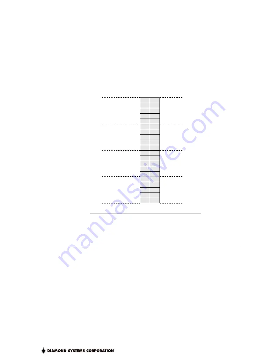
4.14 Serial Port I/O Connector – J18 

J18 is 40-pin header that provides access to the 4 on-board serial ports for Hercules-EBX.  The 
first two serial ports are always configured to meet RS232 standards; the last two serial ports are 
software configurable as either RS232 or RS485.  All four serial ports are independently enabled 
and the last two serial ports can be independently configured between the two modes of operation 
(RS232 versus RS485).   

Diamond Cable Assembly Number 

C-DB9M-4

 connects this header to 4 DE-9 Male connectors 

(for direct connection to RS232C signaling).  The following tables list the signals for the 
appropriate mode of operation, as well as the DE-9 pin numbers to which these signals are wired. 


Port 1 

DCD 1 

DSR 1 

 RXD 

RTS 1 

 TXD 

CTS 1 

 DTR 

RI 1 

 GND 

10 

N/C 

Port 2 

DCD 2 

11  12 

DSR 2 

 RXD 

13  14 

RTS 2 

 TXD 

15  16 

CTS 2 

 DTR 

17  18 

RI 2 

 GND 

19  20 

N/C 

Port 3 

DCD 3 

21  22 

DSR 3 

 RXD 

23  24 

RTS 3 

 TXD 

25  26 

CTS 3 

 DTR 

27  28 

RI 3 

 GND 

29  30 

N/C 

Port 4 

DCD 4 

31  32 

DSR 4 

 RXD 

33  34 

RTS 4 

 TXD 

35  36 

CTS 4 

 DTR 

37  38 

RI 4 

 GND 

39  40 

N/C 

Table 14: J18 – RS232 Serial Port Connector Pinout 


Signal Name 

Definition 

DE-9 Pin 

Direction 


RS-232C: 

DCD 

Data Carrier Detect  

pin 1 

Input 

DSR 

Data Set Ready  

pin 6 

Input 

RXD 

Receive Data  

pin 2 

Input 

RTS 

Request To Send 

pin 7 

Output 

TXD 

Transmit Data 

pin 3 

Output 

CTS 

Clear To Send 

pin 8 

Input 

DTR 

Data Terminal Ready 

pin 4 

Output 

RI 

Ring Indicator 

pin 9 

Input 

N/C Not 

Connected  --- 

---


Summary of Contents for HERCULES-EBX HRC400-5A128

Page 1: ...thernet and Data Acquisition Models HRC400 5A128 HRC550 5A128 HRC550 5N128 HRC750 5A256 User Manual Document 765800 Revision 1 02 Copyright 2003 Diamond Systems Corporation 8430 D Central Ave Newark C...

Page 2: ...4 18 LCD Panel LVDS Interface Connector J24 27 4 19 VGA Connector J25 27 4 20 Video TV Out Connector J26 28 4 21 CPU Fan Connector J27 29 4 22 LCD Backlight Connector J28 29 4 23 Low Voltage Power Inp...

Page 3: ...5 Wait for the conversion to finish 81 12 2 6 Read the data from the board 81 12 2 7 Convert the numerical data to a meaningful value 83 12 3 A D Scan Interrupt and FIFO Operation 84 12 4 Hercules EBX...

Page 4: ...S Table 1 J1 J2 PC 104 Connector Pinouts 11 Table 2 J3 PC 104 Connector Pinout 12 Table 3 J6 PS 2 Connector Pinout 14 Table 4 J7 Utility Connector Pinout 14 Table 5 J8 Data Acquisition DIO Header Pino...

Page 5: ...ble 38 DIO Data and Control Registers Page 0 95 Table 39 DIOCTR0 DIO3 0 Alternate Functions 96 Table 40 DIOCTR1 DIO7 4 Alternate Functions 96 Table 41 DIO Pull Up Down Configuration 98 Table 42 PWM Co...

Page 6: ...nnection system in place of card edge connectors as well as mounting holes for stand offs in each corner The result is an extremely rugged computer system fit for mobile and miniature applications PC...

Page 7: ...d powered USB ports 2 IDE drive connectors standard 40 pin IDE and 44 pin version for notebook drives Accepts solid state flash disk modules directly on board 10 100 BaseT full duplex PCI bus masterin...

Page 8: ...ple FIFO for reliable high speed sampling and scan operation Analog Output 4 analog outputs 12 bit resolution 10V and 0 10V output ranges Simultaneous update Adjustable output range optional Digital I...

Page 9: ...Hercules EBX CPU User Manual V1 02 Page 9 3 HERCULES BOARD DRAWING...

Page 10: ...out 7 310 0 130 in J16 Primary IDE 44 pin laptop 4 833 1 627 in J17 Secondary IDE 40 pin standard 5 060 0 030 in J18 Serial Port I O Connector 2 730 0 030 in J20 External Battery 2 935 1 177 in J21 U...

Page 11: ...end of the PC 104 connector and the board is oriented so that the PC 104 connectors are along the bottom edge of the board View from Top of Board J2 PC 104 16 bit bus connector J1 PC 104 8 bit bus co...

Page 12: ...V SDONE 11 STOP 3 3V LOCK GND 12 3 3V TRDY GND DEVSEL 13 FRAME GND IRDY 3 3V 14 GND AD16 3 3V C BE2 15 AD18 3 3V AD17 GND 16 AD21 AD20 GND AD19 17 3 3V AD23 AD22 3 3V 18 IDSEL0 GND IDSEL1 IDSEL2 19 AD...

Page 13: ...or 2 Use the VIO pins on the PCI edge connector to power the I O drive circuitry or the maximum voltage overshoot protection circuitry on the card From a system perspective the primary question is whi...

Page 14: ...Reset Key Ground 3 4 Power Button Network Activity LED 5 6 3 3V Standby Network 100MBit link 7 8 3 3V Standby 5V In 9 10 IDE LED Power LED 11 12 External Battery Watch Dog Timer Input 13 14 Ground SPE...

Page 15: ...ol is enabled with a jumper on jumper block J4 see page 33 5V This pin is a switched power pin that is turned on and off with the ATX power switch or with the 5V input 3 3V Standby This pin is a speci...

Page 16: ...in addition to connector J20 Note that these two sources are not directly connected and may both be driven by separate external battery power sources Typical power draw from this battery source will a...

Page 17: ...WM3 DIO E4 GATE1 37 38 DIO E5 TOUT1 DIO E6 DIOLATCH 39 40 DIO E7 GATE0 EXTTRIG 41 42 TOUT0 ACK 43 44 WDI WDO 45 46 FXA FXB 47 48 FXB 5V 49 50 Digital Ground Table 5 J8 Data Acquisition DIO Header Pino...

Page 18: ...11 12 Vin 2 Vin 3 13 14 Vin 19 Vin 3 13 14 Vin 3 Vin 4 15 16 Vin 20 Vin 4 15 16 Vin 4 Vin 5 17 18 Vin 21 Vin 5 17 18 Vin 5 Vin 6 19 20 Vin 22 Vin 6 19 20 Vin 6 Vin 7 21 22 Vin 23 Vin 7 21 22 Vin 7 Vin...

Page 19: ...RJ45 For development J10 may be more useful but it is anticipated that most embedded applications will make the J11 connection more useful for panel mount network connection Ensure that only one conn...

Page 20: ...EFT Low 4 Volume MID 5 Line level Mono Output 6 Audio Ground 7 Speaker RIGHT Low 8 Volume HIGH 9 Speaker RIGHT High 10 No Connect Table 9 J13 Amplified Speaker Connector Pinout Signal Name Definition...

Page 21: ...ut to the AC97 Sound circuitry The connector is an industry standard CD IN connector as is common in most desktop Personal Computers Note that the left and right grounds are decoupled but are also tie...

Page 22: ...ound IDEIOR 25 26 Ground IORDY 27 28 Ground DACK 29 30 Ground IRQ14 31 32 Pulled low for 16 bit operation A1 33 34 Not Used A0 35 36 A2 CS0 37 38 CS1 LED 39 40 Ground 5V 41 42 5V Ground 43 44 Not Used...

Page 23: ...header It mates with Diamond Systems UDMA cable no 698026 and may be used to connect up to 2 IDE drives hard disks CD ROMs or other IDE ATAPI devices The 40 pin connector must mate with this 80 condu...

Page 24: ...ignals for the appropriate mode of operation as well as the DE 9 pin numbers to which these signals are wired Port 1 DCD 1 1 2 DSR 1 RXD 1 3 4 RTS 1 TXD 1 5 6 CTS 1 DTR 1 7 8 RI 1 GND 9 10 N C Port 2...

Page 25: ...Ribbon cable header 4 15 External Battery Connector J20 1 Batter input 2 Ground Table 16 J20 External Battery Input The external battery voltage maintains the on board Real Time Clock as well as the o...

Page 26: ...t USB devices to both USB1 on J22 and J23 Connector Part Numbers J21 J22 Connector on CPU board Standard 2x5 0 1 header with pin 1 removed J21 J22 Mating Cable Connector Oupiin 4072 2X5H Standard PC U...

Page 27: ...d J28 below in order to function correctly Signal Name Definition Y Data 2 0 Primary Data Channel bits 2 0 LVDS Differential signaling Y Clock Primary Data Channel Clock LVDS Differential signaling Z...

Page 28: ...header J25 Mating Cable Connector Standard 2x5 0 1 female ribbon cable connector 4 20 Video TV Out Connector J26 1 S Video Y 2 S Video C 3 Composite 4 Ground 5 No Connect Table 21 J26 Video Out Heade...

Page 29: ...nd Table 23 J28 LCD Backlight Connector Pinout Signal Name Definition Control Output signal from Hercules EBX to allow power down of backlight 12V Ground Power Supply for LCD Backlight assembly J28 pr...

Page 30: ...to high current draw and voltage dips encountered due to these current variations Specifically Hard Drives attached to the system may not power up correctly and or may reset Hard Drives CD ROMs and ot...

Page 31: ...an external momentary switch A short press on the switch will turn on power and holding the switch on for 4 seconds or longer will turn off power See Utility Header description for J7 above Diamond Sy...

Page 32: ...ket is to be used it will occupy the entire secondary IDE channel To set the CompactFlash card as an IDE MASTER so that the BIOS detects it place a jumper on J5 as detail on page 35 4 26 OPTIONAL Disk...

Page 33: ...sharing ATX Power Control The ATX power control is set with this jumper block If the ATX jumper is in ATX works normally an external momentary switch may be used to turn power on and off A quick conta...

Page 34: ...Q5 5 AD OR AD IRQ5 4 AD AD IRQ4 AD 7 AD IRQ7 Figure 3 J4 IRQ Jumper Setting Examples Note that COM4 defaults with no hardware IRQ configuration polling mode only ATX IN ATX like Power Control OUT Stan...

Page 35: ...he optional CompactFlash slot on the back of the board is configured to the Secondary IDE Channel As such it can be detected as either a MASTER device or a SLAVE device With no jumper a CompactFlash c...

Page 36: ...value when not otherwise driven DIO Control Lines pulled down data 0 value when not otherwise driven DIO LINES PE4 5 6 7 DIO LINES PE4 5 6 7 Figure 7 J5 DIO Pull Up Pull Down Examples 5 3 J19 PCI VI...

Page 37: ...ly determined by checking the keying of the card 5V card Pin A1 missing pin D30 present 3 3V Card Pin A1 present pin D30 missing Universal Card both pins present The only solution for cards that are i...

Page 38: ...elow J18 is a small square labeled Crisis Recovery which encircles two metal pads on the PCB If these two pads are briefly shorted before and during power up the system will be forced into a System Re...

Page 39: ...ault To use COM4 on the default jumper pinout either COM1 must be disabled changed for access to IRQ3 or the Secondary IDE controller must be disabled for access to IRQ15 Alternatively another IRQ may...

Page 40: ...another PC can be connected to the serial port on Hercules EBX with a null modem cable and a terminal emulation program such as HyperTerminal can be used to establish the connection The terminal prog...

Page 41: ...ings you have made If you erase the CMOS RAM the next time the CPU powers up COM2 will return to the default settings of 115 2Kbaud N 8 1 and operate only during POST If you selected COMA or COMB then...

Page 42: ...max MUX RESET WDO RESET SMI Figure 9 Watchdog Timer Block Diagram The duration of each timer is user programmable When WD1 is triggered it begins to count down When it reaches zero it triggers WD2 set...

Page 43: ...up to the POST screen See the information in the Utilities BIOS Recovery folder of the Hercules EBX files area of the DSC customer CD for instructions on using this program Note that the onboard sett...

Page 44: ...S Settings accessible in the BIOS configuration menus for video which is then removed from use for main system memory This implies that the more memory used for the Video the less memory is available...

Page 45: ...available via J17 40 pin standard UDMA connector Be aware of which channel is which if you are attempting to disable one unused channel in order to free up IRQ resources 32 bit I O settings can be man...

Page 46: ...This setting has no direct affect on PCI or memory speeds it only affects ISA PC 104 devices It is best to leave this setting at Normal if there are no ISA I O Performance issues On the Advanced scre...

Page 47: ...t system 4 Floppy disk should be accessed light on floppy drive starts up and floppy whirs for several seconds if you have a PC speaker attached to the utility header after a few seconds you should he...

Page 48: ...ress Note that the BIOS detects these I O settings and configures COM3 and COM4 I O Addresses accordingly The IRQ s for the two COM parts are manually selectable via jumpers on header J4 see page 34 f...

Page 49: ...g to COM 2 will be enabled regardless of the COM PORT settings elsewhere Continue CR After POST Off default or On o Determines whether the system is to Wait for CR over COM PORT before continuing afte...

Page 50: ...83815 to reach the product folder A DOS utility program is provided for testing the chip and accessing the configuration EEPROM Each board is factory configured for a unique MAC address using this pro...

Page 51: ...485 mode is chosen then special consideration is required to implement RS485 mode in both hardware and software In hardware the critical issues for RS485 mode are 1 No handshaking lines are supported...

Page 52: ...n onboard vertical USB connector J23 located on the top left corner of the board J23 should only be used when USB1 on J22 is not used do not connect USB devices into both connectors or neither device...

Page 53: ...ct the following options a Normal Install b Select the following four options i VIA ATAPI Vendor Support Driver ii AGP VxD Driver iii IRQ Routing Miniport Driver iv VIA INF Driver v1 40a c Install VIA...

Page 54: ...r Windows 2000 and XP 9 2 DOS Operating Systems Installation Issues Installation of DOS operating systems MS DOS FreeDOS ROM DOS should follow the sequence below 1 Enable the following in BIOS a Flopp...

Page 55: ...terrupt rate is reduced by a factor equal to the size of the FIFO threshold enabling a faster A D sampling rate In DOS or similar low overhead operating systems the circuit can operate at sampling rat...

Page 56: ...as follows Page 0 Base Write Function Read Function 0 Reset page register A D LSB 1 Analog configuration register A D MSB 2 A D low channel A D low channel readback 3 A D high channel A D high channe...

Page 57: ...er FPGA Revision Code Page 2 Base Write Function Read Function 24 D A waveform future Feature ID register A D 25 D A waveform future Feature ID register D A 26 D A waveform future Feature ID register...

Page 58: ...A ADSTART 16 DIOA7 DIOA6 DIOA5 DIOA4 DIOA3 DIOA2 DIOA1 DIOA0 17 DIOB7 DIOB6 DIOB5 DIOB4 DIOB3 DIOB2 DIOB1 DIOB0 18 DIOC7 DIOC6 DIOC5 DIOC4 DIOC3 DIOC2 DIOC1 DIOC0 19 DIOD7 DIOD6 DIOD5 DIOD4 DIOD3 DIOD...

Page 59: ...EN CLKSEL CLKEN 14 TINT DINT AINT OVF FF TF EF 15 CFG1 CFG0 ADCH4 ADCH3 ADCH2 ADCH1 ADCH0 16 DIOA7 DIOA6 DIOA5 DIOA4 DIOA3 DIOA2 DIOA1 DIOA0 17 DIOB7 DIOB6 DIOB5 DIOB4 DIOB3 DIOB2 DIOB1 DIOB0 18 DIOC7...

Page 60: ...D5 D4 D3 D2 D1 D0 29 A6 A5 A4 A3 A2 A1 A0 30 EE_EN EE_RW RUNCAL CMUXEN TDACEN PAGE 1 READ Blank bits are unused and read back as 0 Note that offset 31 is the FPGA revision code 0x40 for this product O...

Page 61: ...3 2 1 0 0 HOLDOFF RESET PAGE1 PAGE0 24 25 26 27 28 29 30 PAGE 2 READ Blank bits are unused and read back as 0 Offset 7 6 5 4 3 2 1 0 0 24 ADQ7 ADQ6 ADQ5 ADQ4 ADQ3 ADQ2 ADQ1 ADQ0 25 FDID2 FDID1 FDID0 D...

Page 62: ...annel registers and range settings are cleared to 0 Except for Analog Configuration Register Base 1 which is set to 0x04 D A channels cleared to mid scale or zero scale depending on the board jumper s...

Page 63: ...FF 0 single ended 1 differential A D mode ADBU 0 bipolar 1 unipolar A D input range Note that these signal settings can be read back from Base 4 Base 1 Read A D MSB Register Bit No 7 6 5 4 3 2 1 0 Nam...

Page 64: ...o between the input voltage and the voltage seen by the A D converter The A D always works with a maximum input voltage of 10V A gain of 2 means the maximum input voltage at the connector pin is 5V Ba...

Page 65: ...DA6 DA5 DA4 DA3 DA2 DA1 DA0 DA7 0 D A LSB data Base 7 Write D A MSB Register Bit No 7 6 5 4 3 2 1 0 Name DA15 DA14 DA12 DA12 DA11 DA10 DA9 DA8 DA15 8 D A MSB data Base 8 Read Write FIFO Threshold Reg...

Page 66: ...uration Register Bit No 7 6 5 4 3 2 1 0 Name LED SINGLE DIOCTR1 DIOCTR0 SCINT CLKSRC1 CLKFRQ1 CLKFRQ0 LED Active high simple status bit used to drive external LED active high Default should be high up...

Page 67: ...etween the low and high channels inclusive upon each trigger CLKEN A D hardware clock enable 0 disabled 1 enabled When CLKEN 1 the A D circuit is triggered by the hardware clock selected with CLKSEL b...

Page 68: ...request ADSTART Start an A D conversion after this command ADBUSY 1 until the A D conversion is finished Base 15 Read Hardware Configuration and A D Channel Readback Bit No 7 6 5 4 3 2 1 0 Name CFG1 C...

Page 69: ...pear on DIOE7 4 pins of I O connectors DIOCTR0 0 digital I O lines DIOE3 0 appear on DIOE3 0 pins of I O connectors 1 PWM signals appear on DIOE3 0 pins of I O connectors See Base 12 Configuration Reg...

Page 70: ...1 CTRD20 CTRD19 CTRD18 CTRD17 CTRD16 CTRD23 16MSB for counter timer 0 Counter timer 0 is 24 bits wide and uses all three bytes Counter timer 1 is 16 bits wide and uses only bytes 1 and 2 The bytes may...

Page 71: ...3 2 1 0 Name WDTRIG WDEN WDSMI WDRST WDT 1 WDEDGE WDIEN WDTRIG If this bit is 1 the remaining bits of this register are ignored and instead the watchdog timer A is retriggered i e reloaded with its in...

Page 72: ...Write PWM Data Register LSB Bit No 7 6 5 4 3 2 1 0 Name PWMD7 PWMD6 PWMD5 PWMD4 PWMD3 PWMD2 PWMD1 PWMD0 PWMD7 0 PWM data bits 7 0 Base 25 Write PWM Data Register CSB Bit No 7 6 5 4 3 2 1 0 Name PWMD1...

Page 73: ...ration byte 0 Reserved for future use PWM1 0 Indicates which of the 4 PWM circuits is being accessed CLK Selects internal clock source for both PWM counters 0 10MHz 1 100 KHz POL Selects polarity of o...

Page 74: ...e EEPROM as indicated by the EE_RW bit However if TDACEN is set simultaneously EE_EN is ignored EE_RW Selects read or write operation for the EEPROM 0 Write 1 Read RUNCAL Writing 1 to this bit causes...

Page 75: ...EPROM is being accessed When either signal is 1 do not access the data and address registers at base 12 and base 13 Base 31 Write EEPROM Access Key Register The user must write the value 0xA5 binary 1...

Page 76: ...d by the FPGA FIFO Currently only a value of 001 is defined which describes a FIFO depth of 2048 samples DAQ4 0 Indicates the number of D A channels available on the board Base 26 Read Digital I O Fea...

Page 77: ...to enable software to distinguish between different versions ID15 0 indicates a prototype unreleased version and ID15 1 indicates a released design The current revision code as per this document shoul...

Page 78: ...rential inputs is that only half as many are available since two input pins are required to produce a single differential input Hercules EBX can be configured for either 32 single ended inputs or 16 d...

Page 79: ...e 1 and applies to all inputs In addition you can select a gain setting for the inputs which causes them to be amplified before they reach the A D converter The gain setting is controlled in software...

Page 80: ...ected range Therefore to perform A D conversions on a group of consecutively numbered channels you do not need to write the input channel prior to each conversion For example to read from channels 0 2...

Page 81: ...bit is 0 and the program may read the data Here are examples while inp base 4 0x80 Wait for conversion to finish before proceeding This method could hang your program if there is a hardware fault and...

Page 82: ...he data range always includes both positive and negative values even if the board is set to a unipolar input range The data must now be converted to volts or other engineering units by using a convers...

Page 83: ...alue 32768 Full scale input range Example Input range is 5V and A D value is 17761 Input voltage 17761 32768 5V 2 710V For a bipolar input range 1 LSB 1 32768 Full scale voltage Here is an illustratio...

Page 84: ...rupt would be generated if FIFOEN 1 and ADINTE 1 If the FIFO overflows then the Overflow flag OVF will be set as the 2049th sample is taken In this case the FIFO will not accept any more data and its...

Page 85: ...se 3 5 bit number 0 31 WAIT Page 0 Base 4 bit 6 ADBUSY Page 0 Base 4 bit 7 FIFO threshold Page 0 Base 8 LSB Base 9 MSB CLKEN Page 0 Base 13 bit 0 CLKSEL Page 0 Base 13 bit 1 SCANEN Page 0 Base 13 bit...

Page 86: ...interrupt routine reads one A D sample each time it runs 1 0 1 A D Scans are triggered by the source selected with CLKSEL ADBUSY goes high at the first ADSTS high pulse and stays high until the last A...

Page 87: ...l used interchangeably to mean the conversion of digital data originating from the Hercules EBX computer hardware to an analog signal terminating at an external source 13 2 Resolution The resolution i...

Page 88: ...ode 0 10V Full scale range 10V 0V 10V Desired output voltage 2 000V D A code 2 000V 10V 4096 819 2 819 Note the output code is always an integer For the unipolar output range 0 10V 1 LSB 1 4096 10V 2...

Page 89: ...10V 10V 20V Desired output voltage 2 000V D A code 2V 10V 2048 2048 2457 6 2458 For the bipolar output range 10V 1 LSB 1 4096 20V or 4 88mV Here is an illustration of the relationship between D A code...

Page 90: ...trip off low 8 bits keep 4 high bits Example Output code 1776 LSB 1776 255 240 F0 Hex MSB int 1776 256 int 6 9375 6 The LSB is an 8 bit number in the range 0 255 The MSB is a 4 bit number in the range...

Page 91: ...nt all of the latched data would be enabled through the D A and the analog outputs would begin the transition to the selected values at the same time 13 4 5 WAIT FOR THE D A TO UPDATE Writing the chan...

Page 92: ...DAC Address Page 1 Base 29 Bits 2 0 TrimDAC Address A2 A0 Address for TrimDAC TDACEN Page 1 Base 30 Bit 3 TDACEN TrimDAC Enable when 1 note that this is mutually exclusive with EE_EN control Table 35...

Page 93: ...es 13 6 Analog Circuit Calibration Procedures Calibration applies only to boards with the analog I O circuitry The analog I O circuit is calibrated during production test prior to shipment Over time t...

Page 94: ...ple read one byte from EEPROM location 128 outp base 0 0x01 set page to page 1 outp base 15 0xA5 unlock EEPROM outp base 29 0x80 set address location to 128 0x80 outp base 30 0xC0 Initiate transfer se...

Page 95: ...IRD and DIRE control the direction of ports A B C D and E respectively A 0 means input and a 1 means output All ports power up to input mode and the output registers are cleared to zero When a port di...

Page 96: ...erchangeably the two methods are provided to allow maximum flexibility for output operations 13 9 Special Digital I O Operation Port E In addition to the standard Digital I O operation detailed above...

Page 97: ...transitions from high to low ACK is driven low as soon as latched data is read into the system o Present on DIO Header J8 pin 43 The handshaking sequence would look similar to this over the course of...

Page 98: ...no external source driving the signal Pull down means that a weak 47kOhm pull down resistor will be connected between the DIO signal and ground This sets the DIO signal to a 0 value when there is no...

Page 99: ...Base 13 and Base 27 the counter can be loaded cleared enabled and disabled the optional gate can be enabled and disabled and the counter value can be latched for reading 14 2 Counter 1 Counting Total...

Page 100: ...er 1 Latch the counter The counter continues to operate 2 Read the value from the data registers A counter may be enabled or disabled at any time If disabled the counter will ignore incoming clock edg...

Page 101: ...e 27 0x10 outp base 27 0x90 The counter will run only when the gate input is high Disabling the counter gate Counter 0 Counter 1 outp base 27 0x20 outp base 27 0xA0 The counter will run continuously C...

Page 102: ...witches to the opposite inactive polarity on the next clock CT0 runs continuously When it is 0 on the next clock both counters will reload from their load registers and the cycle will repeat CT0 and C...

Page 103: ...lue for the duty cycle counter counter 1 Counter 1 Value Timer 0 Value Duty Cycle Counter 1 value 10000 0 25 Counter 1 value 2500 d Program the two counters outp base 0 1 Set page 1 for PWM functions...

Page 104: ...register description outp base 0 1 Set page 1 for PWM functions outp base 27 0xA7 Configure and enable PWM output 2 f Finally to enable PWM outputs replacing Digital I O Port E bit3 0 see page 96 set...

Page 105: ...e Watchdog Timer in order to accommodate varying software latencies Interrupt latencies other tasks with priority at certain times etc Setting up the watchdog timer outp base 0 0x00 set page 0 outp ba...

Page 106: ...on the data acquisition header J9 Since software is not involved in maintaining the timer we do can set the reset period to a much smaller value In this example the reset pulse will travel across the...

Page 107: ...6 of full scale Output ranges Unipolar 0 10V or user programmable Bipolar 10V or user programmable Output current 5mA max per channel Settling time 4 S max to 1 2 LSB Relative accuracy 1 LSB Nonlinear...

Page 108: ...32MB flashdisk Multi Sector Transfer Disable LBA Mode Control Enable 32 Bit I O Disable Transfer Mode Fast PIO 1 Ultra DMA Mode Disable Exit the BIOS and save your change The system will now boot and...

Page 109: ...uses systemwide hardware reset Power LED lights when main system power is active note that stand by power may still be active when this LED is off Ethernet 100MBit link LED lights up when 100Mbit link...

Page 110: ...should be off One 50 pin ribbon cable DSC part C 50 18 should be connected from the Hercules EBX board connector J8 to the DAQ test board J3 Note the pin 1 designations on both boards ensure that the...

Page 111: ...nnel 20 2 2 DIO C DIO D DIOE LOOPBACK DIO channel C bits 7 0 is looped back to DIO channel D bits 7 0 and DIO channel E bits 7 0 through some switches for bits 7 4 For basic loopback testing switch ba...

Page 112: ...be used for alternative functions for the DIO interface In addition there are several dedicated signals for some of these special functions See the section 95 for more details GATE 0 This signal is us...

Page 113: ...d TOUT1 should be configured to generate the desired output making sure that DIO Channel E7 4 are configured for alternate functions iii Use DIO A bit 0 to drive EXTTRIG In this case SW1 switch 3 shou...

Page 114: ...Vref H 4 7768V VIN 5 V 9 5536V VIN 6 V 9 5536V VIN 7 Ground 0 V VIN 8 Ground 0 V VIN 9 VOUT 0 buffered VIN 10 VOUT 0 buffered VIN 11 Ground 0 V VIN 12 VOUT 0 buffered VIN 13 VOUT 1 VIN 14 VOUT 2 VIN 1...

Page 115: ...t and readings for VIN9 VIN10 VIN12 VIN13 VIN14 and VIN15 may not be correct depending on whether the output voltage is higher than the associated low side differential voltage for the given input cha...

Page 116: ...e provided for the external hard drive or CD ROM drive A dedicated connector J2 is provided for the flashdisk module Any two devices may be connected simultaneously using this board with proper master...

Page 117: ...7 TV out cable S Video mini DIN and Composite RCA jack output NTSC only 5 698018 Amplified audio output Speaker out with volume control signals with stripped tinned leads 6 698024 VGA Ribbon cable to...

Page 118: ...Hercules EBX CPU User Manual V1 02 Page 118 Figure 14 Hercules EBX Cable Kit...

Page 119: ...ssible that the system boot sequence might be impeded by such conflicts Take care to read through this documentation the section on ISA Resource defaults in particular to familiarize yourself with the...

Page 120: ...120 Alternative heatsinks for low air flow and dusty environments Conformal Coating Jumperless configuration all settings made on board with no jumper headers required See your sales representative fo...

Page 121: ...Hercules EBX CPU User Manual V1 02 Page 121...

Page 122: ...U User Manual V1 02 Page 122 PC 104 Mechanical Drawing The following drawing is from the PC 104 specification This document may be downloaded from www pc104 org or from www diamondsystems com support...

Page 123: ...Hercules EBX CPU User Manual V1 02 Page 123...

Reviews: