Hercules-EBX CPU User Manual V1.02
Page 35
5.2 J5: Data Acquisition Configuration
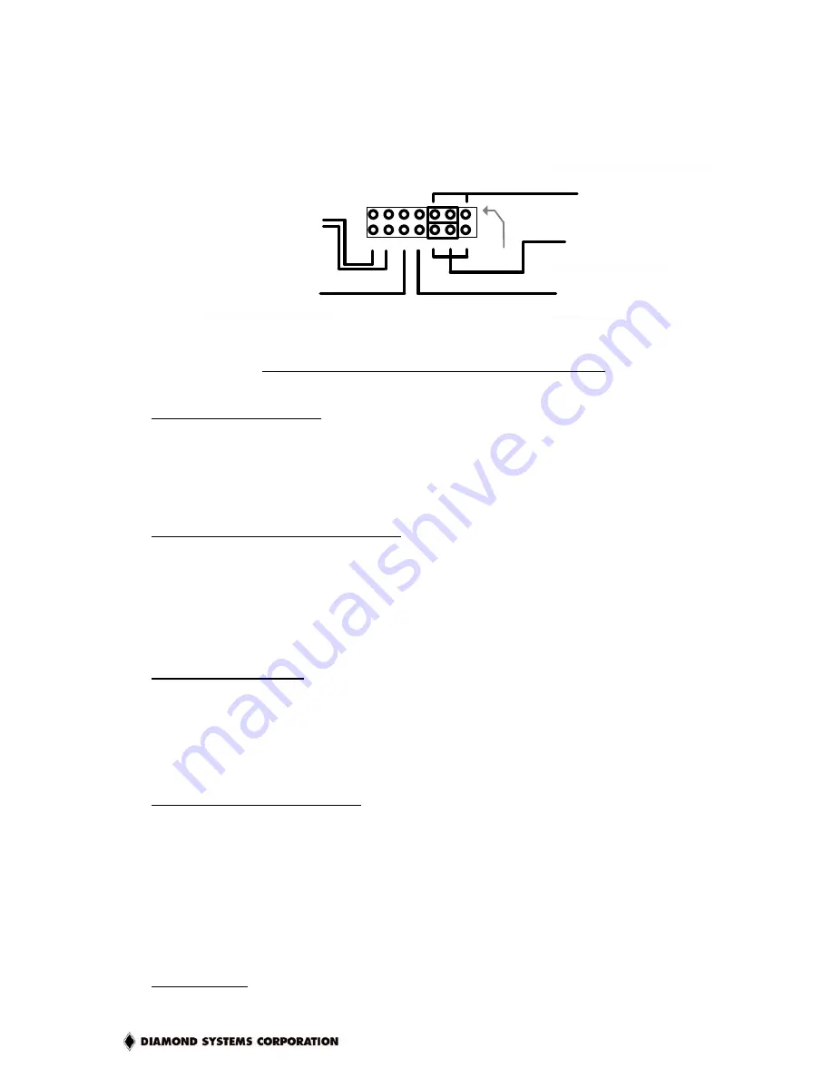
Jumper block J5 is used for configuration of DIO pull-ups/pull-downs, DIO control signal pull-
ups/downs, CompactFlash mode, Flash Write Protect (for boot sector), and COM3/4 Address
Selection.
COM PORT Address Selection:
"B" = COM4 (2E8 * or 3E0)
"A" = COM3 (3E8 * or 2F0)
J5 CONFIG
A
B
CF FW
L
H
DIO
DIO LINES
<PE4,5,6,7
CompactFlash IDE:
Slave*(default) or
Master (jumper)
Write-Protect Flash:
Unprotected * or
Protected (jumper)
DIO Data Lines:
Pull-down (left)* or
Pull-up (right)
DIO Control Lines:
Pull-down (left)* or
Pull-up (right)
Figure 5 : J5 – Data Acquisition Configuration Header
Serial Port Address Settings
COM3 may be set to either I/O address 0x03E8 (no jumper) or 0x02F8 (jumper added to “A”
position on J5). Similarly, COM4 may be set to either I/O address 0x02E8 (no jumper) or 0x03E0
(jumper added to “A” position on J5). These settings are immediately in effect, but the BIOS must
start with these jumpers in position in order to automatically detect and configure the ports
correctly. Change these settings only while the system is powered down.
CompactFlash IDE Control <OPTIONAL>
The optional CompactFlash slot on the back of the board is configured to the Secondary IDE
Channel. As such, it can be detected as either a MASTER device or a SLAVE device. With no
jumper, a CompactFlash card would be detected as a SLAVE device. With this jumper, the
CompactFlash will be a MASTER IDE Device. Note that a SLAVE device requires a MASTER
device on the same IDE channel in order to function.
Write-Protect BIOS Flash
Adding this jumper forces protection of the boot-sector of the BIOS Flash. This allows for
dynamic Crisis Recovery in the case where the BIOS PROM becomes corrupted. Note that this
option may not be user-selectable – write Protection may be enforced regardless of this jumper
selection.
DIO Pull-up / Pull-Down Selections
The Digital I/O lines in the Data Acquisition section are broken into two blocks: General Purpose
DIO lines (DIO channels A-D, and Channel E bits 3-0), and Multiplexed Control lines (DIO
Channel E bits 7-4).
The top three pins allow for a pull-down (left) or pull-up (right) selection for the General-Purpose
pins. The bottom three pins allow a similar selection for the multiplexed control lines. This allows
these alternate-function pins to be selected separately since their function may require a different
default state than that provided to the standard digital I/O lines.
Default Settings


