background image

The ConnectCore 8X System-on-module

Wireless interfaces

ConnectCore® 8X System-on-Module Hardware Reference Manual

21

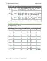
BOOT_MODE
[3]

BOOT_MODE
[2]

BOOT_MODE
[1]

BOOT_MODE
[0]

Boot mode

0

0

0

1

USB serial download

0

0

1

0

USDHC Boot: eMMC0

0

0

1

1

USDHC Boot: USDHC1

0

1

0

0

NAND Boot: 128 pages in
Block

0

1

0

1

NAND Boot: 32 pages in Block

0

1

1

0

FlexSPI Boot: 3B read

0

1

1

1

FlexSPI Boot: Hyperflash 3.0

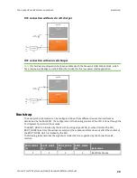
These BOOT_MODE lines are referred to the VCC_SCU_1V8 power domain. By default, none of them
are configured inside the module. To configure the desired boot mode, they must be driven low or
high in the carrier board in the following way:

n

To set high level, place a 4.7K pull-up to VCC_SCU_1V8.

n

To set low level, place a 100K pull-down to GND.

Wireless interfaces

The ConnectCore 8X System-on-module combines a wireless local area network (WLAN) and
Bluetooth dual solution to support MIMO 2x2 IEEE802.11 a/b/g/n/ac WLAN standards and Bluetooth
5.0, enabling seamless integration of WLAN/Bluetooth and Low Energy technology.

WLAN IEEE 802.11a/b/g/n/ac

The 2.4 GHz band on the ConnectCore 8X module supports 20/40 MHz bandwidths, and the 5 GHz
band supports 20/40/80 MHz bandwidths. The following sections specify the performance of the WLAN
IEEE 802.11a/b/g/n/ac interface on the ConnectCore 8X module.

Modulation and data rates

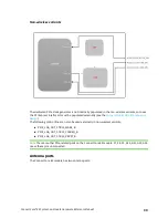
The following tables list modulation values for the ConnectCore 8X module, which supports the
following WLAN standards:

Mode

Modulation & coding Rate

802.11b

DBPSK

1 Mbps

DQPSK

2 Mbps

CCK

5.5 Mbps

CCK

11 Mbps

Summary of Contents for ConnectCore 8X

Page 1: ...ConnectCore 8X System on module Hardware Reference Manual...

Page 2: ...d updated AH13 added RTC mode power consumption use case fix error in Japan radio marking label combined pinout tables clarified power domains comment pad F2 Trademarks and copyright Digi Digi Interna...

Page 3: ...teps to reproduce Contact Digi technical support Digi offers multiple technical support plans and service packages Contact us at 1 952 912 3444 or visit us at www digi com support Feedback To provide...

Page 4: ...tics 17 System power up sequence 19 RTC power and coin cell charger 19 Bootstrap 20 Wireless interfaces 21 WLAN IEEE 802 11a b g n ac 21 Bluetooth 28 PCI Express 28 Antenna ports 30 CryptoAuthenticati...

Page 5: ...MT pick and place 104 SMT process parameter reference 104 Reflow profile 104 Regulatory information and certifications United States FCC 107 Labeling requirements 107 Maximum power and frequency speci...

Page 6: ...is based on the i MX 8X processor from NXP This processor offers a number of interfaces some of them multiplexed and not available simultaneously The module has the following features n i MX 8X dual q...

Page 7: ...and NIST certifiable HMAC based DRBG l RSA up to 4096 Elliptic Curve up to 1023 l AES 128 192 256 DES 3DES ARC4 MD5 SHA 1 SHA 224 256 384 512 l Dedicated Security Controller for Flashless SHE and HSM...

Page 8: ...itself is not used o 4x I2C High Speed DMA support One of them I2C0 is used internally in the SOM and is not available for general purposes o 4x I2C Low Speed no DMA support o 1x I2C PMIC control ded...

Page 9: ...with debouncing configuration l 9 analog to digital converters ADCs all with comparator capabilities l Watchdog l Tamper detection both digital and analog l 8 bytes of non volatile storage NVRAM l 3...

Page 10: ...About the ConnectCore 8X Block diagrams ConnectCore 8X System on Module Hardware Reference Manual 10 ConnectCore 8X module...

Page 11: ...SOM uses an NXP i MX8X system on chip SOC NXP released two revisions of the system on chip SOC silicon n Revision B0 n Revision C0 On the C0 revision of the i MX8X NXP fixed most of the errata that w...

Page 12: ...ion of the ConnectCore 8X SOM The following table correlates the ConnectCore 8X SOM revision with the i MX8X SOC revision SOM revision Description i MX8X SOC revision 1P 2P Pre production series B0 A...

Page 13: ...X System on module This section describes the functionality of the ConnectCore 8X System on module Power interfaces Reference power architecture scheme The following diagram represents the full power...

Page 14: ...rnal circuitry These additional regulators are not mandatory The following table summarizes the PMIC regulators of the ConnectCore 8X SOM PMIC regulator SoM power rail name Input power supply Internal...

Page 15: ...ut power rail Instead follow the configuration explained in RTC power and coin cell charger In addition to the input power supplies of the PMIC other power domains of the SOM must also be set external...

Page 16: ...n VDD_CSI_1P8_3P3 Input power supply for CSI interface USB_OTG1_VBUS i MX 8X CPU USB_OTG1_VBUS Input power supply for the USB1 interface VBUS Note The CPU input power rails on the table above power di...

Page 17: ...e V Minimum Typical Maximum PMIC VSYS TBD 3 7 5 5 VSYS2 TBD 3 0 5 5 LDO3IN 2 51 5 5 LDO4IN 2 51 5 5 MCA VCC_MCA TBD 1 71 3 6 CPU VDD_USDHC1 VDD_MIPI_DSI_DIG VDD_ENET0 VDD_SPI_SAI VDD_QSPI0B VDD_CSI 1...

Page 18: ...00 2500 LD02 VDD_EMMC0 YES 3 30 3 0 3 0 400 500 2500 LD03 LDO3 NO 1 5 5 0 3 0 3 0 400 500 2500 LD04 LDO4 NO 1 5 5 0 3 0 3 0 400 500 2500 VSNVS VCC_ LICELL coin cell charger 2 6 V to 3 6 V YES 1 8 3 6...

Page 19: ...inally the CPU reset line which is controlled by both the PMIC and the MCA is released The following time diagram shows the power up sequence RTC power and coin cell charger The VCC_LICELL pin support...

Page 20: ...be configured to boot from different devices and interfaces as determined by the Boot ROM The configuration of the booting process of the CPU is done through the SCU System Control Unit boot mode The...

Page 21: ...K pull up to VCC_SCU_1V8 n To set low level place a 100K pull down to GND Wireless interfaces The ConnectCore 8X System on module combines a wireless local area network WLAN and Bluetooth dual solutio...

Page 22: ...QAM 1 2 24 Mbps 16QAM 3 4 36 Mbps 64QAM 2 3 48 Mbps 64QAM 3 4 54 Mbps 802 11n BPSK 1 2 MCS0 QPSK 1 2 MCS1 QPSK 3 4 MCS2 16QAM 1 2 MCS3 16QAM 3 4 MCS4 64QAM 2 3 MCS5 64QAM 3 4 MCS6 64QAM 5 6 MCS7 802 1...

Page 23: ...90 175 5 195 5 64 QAM 2 3 52 57 8 108 120 234 260 6 64 QAM 3 4 58 5 65 121 5 135 263 3 292 5 7 64 QAM 5 6 65 72 2 135 150 292 5 325 8 256 QAM 3 4 78 86 7 162 180 351 390 9 256 QAM 5 6 180 200 390 433...

Page 24: ...20 100 5500 104 5520 108 5540 112 5560 116 5580 120 5600 124 5620 128 5640 132 5660 136 5680 140 5700 144 5720 149 5745 153 5765 157 5785 161 5805 165 5825 40 MHz 40 MHz 38 5190 46 5230 54 5270 62 531...

Page 25: ...DFS TPC 100 5500 DFS TPC DFS DFS DFS TPC 104 5520 DFS TPC DFS DFS DFS TPC 108 5540 DFS TPC DFS DFS DFS TPC 112 5560 DFS TPC DFS DFS DFS TPC 116 5580 DFS TPC DFS DFS DFS TPC 120 5600 DFS TPC DFS No Ac...

Page 26: ...ivity The following table lists typical receive sensitivity values for the ConnectCore 8X module Mode 802 11b 802 11ga 802 11n 802 11ac Modulation DBPSK CCK BPSK 1 2 64QAM 3 4 BPSK 1 2 64QAM 5 6 BPSK...

Page 27: ...or each antenna individually so in MIMO applications the total output power will be the sum of both antennas FCC RF band Channel BW Standard Output power dBm 2 4 GHz 20 MHz 802 11b 13 5 20 MHz 802 11g...

Page 28: ...rd in the 5 GHz band Bluetooth The ConnectCore 8X module supports both Bluetooth and Bluetooth Low Energy protocols n Bluetooth 5 0 backwards compatible with Bluetooth 1 X 2 X Enhanced Data Rate Bluet...

Page 29: ...ConnectCore 8X System on Module Hardware Reference Manual 29 Wireless variants...

Page 30: ...populated externally see the ConnectCore 8X SBC Pro reference design The following control lines can also be used externally in non wireless variants n PCIE_LGA_OUT_CTRL0_WAKE_B n PCIE_LGA_OUT_CTRL0_...

Page 31: ...urve support n SHA 256 hash algorithm with HMAC option n 256 bit key length n Storage for up to 16 keys n Two high endurance monotonic counters n Guaranteed unique 72 bit serial number n Internal High...

Page 32: ...with the PMIC controls the reset line of the i MX 8X processor The SYS_ RESET pin is the main reset input of the ConnectCore 8X module This pin is a pseudo open drain with an internal pull up Assertin...

Page 33: ...even if the MCA releases the reset line before the PMIC is ready the CPU won t go out of reset The following time diagram represents the reset sequence Default values are as follows n tr1 50 ms n tr2...

Page 34: ..._IO3 AN23 54 MCA_IO4 AL27 61 MCA_IO5 AL28 62 MCA_IO6 AK29 63 MCA_IO7 AJ29 64 MCA_IO8 AH29 65 MCA_IO9 AG29 66 MCA_IO10 AF29 67 MCA_IO11 AM26 MCA_IO12 AM25 MCA_IO13 AL22 MCA_IO14 AL26 MCA_IO15 AL25 MCA_...

Page 35: ...DC lines to act as an analog window comparator and generate an IRQ depending on the voltage level in the input This feature allows applications to be notified of this event instead of needing to perio...

Page 36: ...A RTC is preferred due to its superior power consumption efficiency To preserve the date during power off you must connect a coin cell battery following the design notes provided in System on module p...

Page 37: ...ows x 8 columns The controller detects each key press and release and implements a configurable debounce filter that prevents the detection of undesirable events caused by switch bouncing Additionally...

Page 38: ...guration through device tree and access through sysfs Note See the ConnectCore 8X software documentation for additional information about how to configure the LED and how to assign that functionality...

Page 39: ...re ConnectCore 8X System on Module Hardware Reference Manual 39 W4PK mode You can configure boot mode using the mca_config_tool boot_mode option If boot on power BOP is chosen the module will enter in...

Page 40: ...n The MCA goes into sleep mode keeping active the peripherals that always run in low power modes like the RTC and those configured to wake up the system such as IRQs and power IO MCA GPIOs configured...

Page 41: ...cally set the OFF state unless the user explicitly cancels it by writing to the mca_ cancel_pwroff entry in the sysfilesystem MCA_VIN_DET signal The on module MCA is powered from a dedicated external...

Page 42: ...simplify pin configuration and resolution You can enter the list of interfaces required by your project and use the Smart IOmux graphical interface to mock up configuration options resulting in full...

Page 43: ...Module pinout The ConnectCore 8X System on module has a mixed pad structure It provides 474 LGA pads and 118 peripheral castellated pads The general layout can be found on the following diagram Note T...

Page 44: ...ground n Never drive an I O pin from an external power source during the power on or reset sequences n Never hot swap the module or interrupt its ground connection to external circuitry Latch up is a...

Page 45: ...CD_B USDHC1_CD_B ALT0 USDHC1_CD_B ALT1 NAND_DQS_P ALT2 SPI2_CS0 ALT3 NAND_DQS ALT4 GPIO4_IO22 VDD_USDHC1 5 F1 USDHC1_CMD USDHC1_CMD ALT0 USDHC1_CMD ALT1 NAND_CE0_B ALT2 MQS_R ALT3 ALT4 GPIO4_IO24 VDD_...

Page 46: ...TA3 ALT0 USDHC1_DATA3 ALT1 NAND_ALE ALT2 UART3_RTS_B ALT3 ALT4 GPIO4_IO28 VDD_USDHC1 10 L1 USDHC1_CLK USDHC1_CLK ALT0 USDHC1_CLK ALT1 ALT2 UART3_RX ALT3 ALT4 GPIO4_IO23 VDD_USDHC1 11 M1 GND 12 N1 VDD_...

Page 47: ..._SDA ALT1 MIPI_DSI1_GPIO0_IO03 ALT2 ALT3 ALT4 GPIO1_IO26 VDD_MIPI_DSI_DIG 19 Y1 MIPI_DSI0_GPIO0_00 MIPI_DSI0_GPIO0_00 ALT0 MIPI_DSI0_GPIO0_IO00 ALT1 I2C1_SCL ALT2 MIPI_DSI0_PWM0_OUT ALT3 ALT4 GPIO1_IO...

Page 48: ...MIPI_DSI1_GPIO0_IO00 ALT1 I2C2_SCL ALT2 MIPI_DSI1_PWM0_OUT ALT3 ALT4 GPIO1_IO31 VDD_MIPI_DSI_DIG 24 AE1 MIPI_DSI1_GPIO0_01 MIPI_DSI1_GPIO0_01 ALT0 MIPI_DSI1_GPIO0_IO01 ALT1 I2C2_SDA ALT2 ALT3 ALT4 GP...

Page 49: ...I0A_SS0_B ALT1 ALT2 ALT3 ALT4 GPIO3_IO14 3V3 37 AN6 MIPI_DSI0_CLK_N MIPI_DSI0_CLK_N NVCC_MIPI_CSI_DSI 38 AN7 MIPI_DSI0_CLK_P MIPI_DSI0_CLK_P NVCC_MIPI_CSI_DSI 39 AN8 GND 40 AN9 MIPI_DSI0_DATA0_N MIPI_...

Page 50: ...CC_MIPI_CSI_DSI 50 AN19 MIPI_DSI0_DATA3_P MIPI_DSI0_DATA3_P NVCC_MIPI_CSI_DSI 51 AN20 GND 52 AN21 MCA_IO1 ALT0 ADC0_DP1 ADC0_SE1 ALT1 PTE16 ALT2 SPI0_PCS0 ALT3 UART2_TX ALT4 TPM_CLKIN0 ALT5 ALT6 FXIO0...

Page 51: ...lexing Power group Comments 55 AN24 SWD_CLK PWR_IO ALT0 ALT1 PTA0 ALT2 ALT3 TPM0_CH5 ALT4 ALT5 ALT6 ALT7 SWD_CLK VCC_MCA Input power ON OFF line of the module active low 56 AN25 SYS_RESET VCC_MCA Inpu...

Page 52: ...tiplexing Power group Comments 61 AL27 MCA_IO4 ALT0 ADC0_DM2 ADC0_SE6a ALT1 PTE19 ALT2 SPI0_MISO ALT3 ALT4 I2C0_SCL ALT5 SPI0_MOSI ALT6 FXIO0_D3 ALT7 VCC_MCA 62 AL28 MCA_IO5 ALT0 ADC0_DP0 ADC0_SE0 ALT...

Page 53: ...i MX 8X pin name Multiplexing Power group Comments 64 AJ29 MCA_IO7 ALT0 ADC0_DP3 ADC0_SE3 ALT1 PTE22 ALT2 ALT3 TPM2_CH0 ALT4 UART2_TX ALT5 ALT6 FXIO0_D6 ALT7 VCC_MCA 65 AH29 MCA_IO8 ALT0 ADC0_DM3 ADC...

Page 54: ...ALT5 ALT6 ALT7 VCC_MCA 68 AE29 SCU_BOOT_MODE0 SCU_BOOT_MODE0 VCC_SCU_1V8 69 AD29 SCU_BOOT_MODE1 SCU_BOOT_MODE1 VCC_SCU_1V8 70 AC29 SCU_GPIO0_00 SCU_GPIO0_00 ALT0 SCU_GPIO0_IO00 ALT1 SCU_UART0_RX ALT2...

Page 55: ...2_RX UART2_RX ALT0 UART2_RX ALT1 FTM_CH0 ALT2 FLEXCAN1_RX ALT3 ALT4 GPIO1_IO24 3V3 76 U29 FLEXCAN2_RX FLEXCAN2_RX ALT0 FLEXCAN2_RX ALT1 SAI3_RXD ALT2 UART3_RX ALT3 SAI1_RXFS ALT4 GPIO1_IO19 3V3 77 T29...

Page 56: ...0_RTS_B ALT3 SAI1_TXC ALT4 GPIO1_IO15 3V3 81 M29 FLEXCAN0_TX FLEXCAN0_TX ALT0 FLEXCAN0_TX ALT1 SAI2_RXD ALT2 UART0_CTS_B ALT3 SAI1_TXFS ALT4 GPIO1_IO16 3V3 82 L29 ADC_IN1 ADC_IN1 ALT0 ADC_IN1 ALT1 M40...

Page 57: ...VSYNC ALT3 SPI2_SDI ALT4 GPIO0_IO19 3V3 88 E29 MCLK_IN1 MCLK_IN1 ALT0 MCLK_IN1 ALT1 I2C3_SDA ALT2 LCDIF_EN ALT3 SPI2_SCK ALT4 LCDIF_D17 3V3 89 F28 SPI3_CS1 SPI3_CS1 ALT0 SPI3_CS1 ALT1 I2C3_SCL ALT2 LC...

Page 58: ...5 VDD_ENET0 VDD_ENET0 96 A24 ENET0_RGMII_TXC ENET0_RGMII_TXC ALT0 ENET0_RGMII_TXC ALT1 ENET0_RCLK50M_OUT ALT2 ENET0_RCLK50M_IN ALT3 NAND_CE1_B ALT4 GPIO4_IO29 VDD_ENET0 97 A23 ENET0_RGMII_TX_ CTL ENET...

Page 59: ...ET0_RGMII_TXD3 ALT0 ENET0_RGMII_TXD3 ALT1 MLB_SIG ALT2 NAND_RE_B ALT3 ALT4 GPIO5_IO02 VDD_ENET0 102 A18 ENET0_RGMII_RXC ENET0_RGMII_RXC ALT0 ENET0_RGMII_RXC ALT1 MLB_DATA ALT2 NAND_WE_B ALT3 USDHC1_CL...

Page 60: ...NET0 107 A13 ENET0_RGMII_RXD3 ENET0_RGMII_RXD3 ALT0 ENET0_RGMII_RXD3 ALT1 ALT2 NAND_ALE ALT3 USDHC1_DATA3 ALT4 GPIO5_IO08 VDD_ENET0 108 A12 ENET0_REFCLK_ 125M_25M ENET0_REFCLK_125M_ 25M ALT0 ENET0_REF...

Page 61: ...wer group Comments 113 A7 USB_OTG1_P USB_OTG1_DP 3V3 114 A6 USB_OTG1_N USB_OTG1_DN 3V3 115 GND 116 B6 USB_OTG1_VBUS USB_OTG1_VBUS 117 D4 GND 118 C6 USB_OTG1_ID USB_OTG1_ID 3V3 LGA signals and multiple...

Page 62: ...USB_SS3_RX_P USB_SS3_RX_P 1V8 B14 GND B15 GND B16 WLAN_RF_KILL 3V3_RF B17 BT_RF_KILL 3V3_RF B18 GND B19 ESAI0_SCKR ESAI0_SCKR ALT0 ESAI0_SCKR ALT1 ALT2 LCDIF_D02 ALT3 ENET1_RGMII_TX_CTL ALT4 GPIO0_IO...

Page 63: ...up Comments B22 ESAI0_TX1 ESAI0_TX1 ALT0 ESAI0_TX1 ALT1 ALT2 LCDIF_D05 ALT3 ENET1_RGMII_RXD3 ALT4 GPIO0_IO05 VDD_ESAI_SPDIF B23 RESERVED B25 GND B26 GND B27 GND C2 GND C3 RESERVED C4 GND C5 GND C7 USB...

Page 64: ...TC2 USB_SS3_TC2 ALT0 I2C1_SDA ALT1 USB_OTG1_OC ALT2 USB_OTG2_OC ALT3 ALT4 GPIO4_IO05 3V3 C10 USB_OTG2_ID USB_OTG2_ID 3V3 C11 USB_SS3_TC3 USB_SS3_TC3 ALT0 I2C1_SDA ALT1 USB_OTG2_OC ALT2 ALT3 ALT4 GPIO4...

Page 65: ..._TX2_RX3 ALT0 ESAI0_TX2_RX3 ALT1 ENET1_RMII_RX_ER ALT2 LCDIF_D06 ALT3 ENET1_RGMII_RXD2 ALT4 GPIO0_IO06 VDD_ESAI_SPDIF C21 ESAI0_FST ESAI0_FST ALT0 ESAI0_FST ALT1 MLB_CLK ALT2 LCDIF_D01 ALT3 ENET1_RGMI...

Page 66: ...MX 8X pad name Multiplexing Power Group Comments D1 RESERVED D2 GND D3 GND D5 WLAN_SD1_D3 3V3_RF This SDIO interface is connected to the Wireless chip on the wireless variants of the SOM By default t...

Page 67: ...V3_RF D11 WLAN_SD1_CMD 3V3_RF D12 WLAN_SD1_CLK 3V3_RF D13 WLAN_SD1_D5 3V3_RF D14 WLAN_SD1_D4 3V3_RF D15 VDD_ENET0 VDD_ENET0 D16 GND D17 SPI0_SCK SPI0_SCK ALT0 SPI0_SCK ALT1 SAI0_TXC ALT2 M40_I2C0_SCL...

Page 68: ...D21 SPDIF0_RX SPDIF0_RX ALT0 SPDIF0_RX ALT1 MQS_R ALT2 LCDIF_D10 ALT3 ENET1_RGMII_RXD0 ALT4 GPIO0_IO10 VDD_ESAI_SPDIF D22 ESAI0_TX0 ESAI0_TX0 ALT0 ESAI0_TX0 ALT1 MLB_DATA ALT2 LCDIF_D04 ALT3 ENET1_RG...

Page 69: ...ND D29 GND E1 GND E2 GND E5 VDD_EMMC0 VDD_EMMC0 Do not use this power rail unless otherwise noted E6 GND E7 RESERVED E8 GND E9 GPS_COEX 3V3_RF E10 LTE_PRI 3V3_RF E11 LTE_SYNC 3V3_RF E12 BT_UART1_RX UA...

Page 70: ...3_RF Internal UART line used by the Bluetooth This signal is externally available only in non wireless variants E14 VDD_ESAI_SPDIF VDD_ESAI_SPDIF E15 GND E16 VDD_SPI_SAI VDD_SPI_SAI E17 SPI2_SCK SPI2_...

Page 71: ...AI0_RXD ALT0 SAI0_RXD ALT1 SAI1_RXFS ALT2 SPI1_CS0 ALT3 LCDIF_D20 ALT4 GPIO0_IO27 VDD_SPI_SAI E22 SPI0_SDI SPI0_SDI ALT0 SPI0_SDI ALT1 SAI0_TXD ALT2 M40_TPM0_CH0 ALT3 M40_GPIO0_IO02 ALT4 GPIO1_IO05 VD...

Page 72: ...CS1 ALT0 SPI0_CS1 ALT1 SAI0_RXC ALT2 SAI1_TXD ALT3 LCDIF_PWM0 ALT4 GPIO1_IO07 VDD_SPI_SAI F2 VDD_PCIE_DIG VDD_PCIE_DGI 3V3_RF On non wireless variants VDD_ PCIE_DIG must be powered externally in order...

Page 73: ...his signal is externally available only in non wireless variants F6 PCIE_LGA_OUT_CTRL0_ PERST_B ALT0 PCIE_CTRL0_PERST_B ALT4 GPIO4_IO00 VDD_PCIE_DIG Internal PCIe line used by the wireless This signal...

Page 74: ...t drive this signal externally F11 BT_UART1_RTS UART1_RTS_B ALT0 UART1_RTS_B ALT1 PWM2_OUT ALT2 LCDIF_D16 ALT3 GPT1_CAPTURE ALT4 GPTO_CLK 3V3 3V3_RF Internal UART line used by the Bluetooth This signa...

Page 75: ...wer Group Comments F16 GND F17 3V3_RF 3V3_RF F18 3V3_RF 3V3_RF F19 RESERVED F20 RESERVED F21 GND F22 GND F23 QOW 3V3_RF F24 WLAN_LED 3V3_RF Functionality not supported F25 BT_LED 3V3_RF Functionality...

Page 76: ...IO3_IO11 3V3_RF In wireless variants of the SOM this is a reserved output line Do not drive this signal externally G3 PCIE0_LGA_IN_REFCLK_N 1V G4 PCIE0_LGA_IN_REFCLK_P 1V8 G5 GND G6 PCIE0_LGA_OUT_RX0_...

Page 77: ...GND G9 PCIE0_LGA_OUT_TX0_N 1V8 Internal PCIe line used by the Wireless This signal is externally available only in non wireless variants G10 PCIE0_LGA_OUT_TX0_P 1V8 Internal PCIe line used by the Wire...

Page 78: ...ments G18 WLAN_SDIO_INT_L 3V3_RF G19 GND G20 PCIE0_LGA_IN_TX0_P 1V8 Leave this pin floating unless otherwise noted G21 PCIE0_LGA_IN_TX0_N 1V8 Leave this pin floating unless otherwise noted G22 GND G23...

Page 79: ...Hardware Reference Manual 79 LGA pad name ConnectCore 8X signal name i MX 8X pad name Multiplexing Power Group Comments H4 GND H5 GND H6 GND H7 GND H8 GND H9 GND H10 GND H11 GND H12 GND H13 GND H14 G...

Page 80: ...are Reference Manual 80 LGA pad name ConnectCore 8X signal name i MX 8X pad name Multiplexing Power Group Comments H24 GND H25 GND H26 GND H27 GND H28 GND AF2 GND AF3 GND AF4 GND AF5 GND AF6 GND AF7 G...

Page 81: ...Hardware Reference Manual 81 LGA pad name ConnectCore 8X signal name i MX 8X pad name Multiplexing Power Group Comments AF17 GND AF18 GND AF19 GND AF20 GND AF21 GND AF22 GND AF23 GND AF24 GND AF25 GND...

Page 82: ...TA1 ALT0 QSPI0B_DATA1 ALT1 QSPI1A_DATA1 ALT2 KPP0_COL2 ALT3 ALT4 GPIO3_IO19 VDD_QSPI0B AG10 QSPI0B_SS1_B QSPI0B_SS1_B ALT0 QSPI0B_SS1_B ALT1 QSPI1A_SS1_B ALT2 KPP0_ROW3 ALT3 ALT4 GPIO3_IO24 VDD_QSPI0B...

Page 83: ...COL3 ALT3 ALT4 GPIO3_IO20 VDD_QSPI0B AG15 QSPI0B_SCLK QSPI0B_SCLK ALT0 QSPI0B_SCLK ALT1 QSPI1A_SCLK ALT2 KPP0_COL0 ALT3 ALT4 GPIO3_IO17 VDD_QSPI0B AG16 GND AG17 VDD_QSPI0B VDD_QSPI0B AG18 IMX8_ON_OFF...

Page 84: ...0_TPM_CH0 ALT2 M40_GPIO0_IO04 ALT3 ALT4 GPIO1_IO14 1V8 AG26 ADC_IN3 ADC_IN3 ALT0 ADC_IN3 ALT1 M40_UART0_TX ALT2 M40_GPIO0_IO03 ALT3 MCLK_OUT0 ALT4 GPIO1_IO11 1V8 AG27 ADC_IN2 ADC_IN2 ALT0 ADC_IN2 ALT1...

Page 85: ...B VCC_SCU_1V8 Reset signal of the CPU Digi recommends leaving this pin floating 10K pull up inside the module connected to VCC_SCU_1V8 AH11 PMIC_EWARN AH12 PMIC_WDI AH13 VLDO2_VSELECT Leave this pin f...

Page 86: ...CSI_D08 ALT1 ALT2 SAI3_RXC ALT3 TAMPER_IN1 ALT4 VDD_CSI AH21 GND AH22 CSI_PCLK CSI_PCLK ALT0 CSI_PCLK ALT1 MIPI_CSI0_I2C0_SCL ALT2 ALT3 SPI1_SCK ALT4 GPIO3_IO00 VDD_CSI AH23 CSI_VSYNC CSI_VSYNC ALT0 C...

Page 87: ...l name i MX 8X pad name Multiplexing Power Group Comments AH26 CSI_D01 CSI_D01 ALT0 CSI_D03 ALT1 ALT2 SAI0_RXD ALT3 TAMPER_OUT1 ALT4 VDD_CSI AH27 JTAG_TDI JTAG_TDI VCC_SCU_1V8 AH28 JTAG_TMS JTAG_TMS V...

Page 88: ...l of the SOM n ON high level n OFF low level 2 2M pull up on module connected to VCC_MCA AJ13 VCC_SNVS_LDO_1V8 VCC_SNVS_LDO_1V8 Do not use this cell unless otherwise noted AJ14 GND AJ15 MIPI_DSI1_DATA...

Page 89: ...ALT4 GPIO3_IO01 VDD_CSI AJ22 CSI_D07 CSI_D07 ALT0 CSI_D09 ALT1 ALT2 SAI3_RXD ALT3 TAMPER_IN2 ALT4 VDD_CSI AJ23 CSI_D04 CSI_D04 ALT0 CSI_D06 ALT1 ALT2 SAI2_RXD ALT3 TAMPER_OUT4 ALT4 VDD_CSI AJ24 CSI_D...

Page 90: ...D AK7 GND AK8 GND AK9 GND AK10 GND AK11 GND AK12 GND AK13 GND AK14 GND AK15 MIPI_DSI1_DATA1_N MIPI_DSI1_DATA1_N NVCC_MIPI_CSI_DSI AK16 MIPI_DSI1_DATA1_P MIPI_DSI1_DATA1_P NVCC_MIPI_CSI_DSI AK17 GND AK...

Page 91: ...O03 ALT2 ALT3 ALT4 GPIO3_IO06 1V8 AK25 MIPI_CSI0_I2C0_SCL MIPI_CSI0_I2C0_SCL ALT0 MIPI_CSI0_I2C0_SCL ALT1 MIPI_CSI0_GPIO0_IO02 ALT2 ALT3 ALT4 GPIO3_IO05 1V8 AK26 CSI_RESET CSI_RESET ALT0 CSI_RESET ALT...

Page 92: ...SYS AL8 VSYS VSYS AL9 GND AL10 GND AL11 GND AL12 MIPI_CSI0_DATA1_P MIPI_CSI0_DATA1_P NVCC_MIPI_CSI_DSI AL13 MIPI_CSI0_DATA1_N MIPI_CSI0_DATA1_N NVCC_MIPI_CSI_DSI AL14 GND AL15 MIPI_CSI0_DATA0_P MIPI_C...

Page 93: ...32K ALT2 SPI1_MISO ALT3 LPUART1_TX ALT4 RTC_CLKOUT ALT5 CMP0_OUT ALT6 I2C1_SDA ALT7 VCC_MCA AL22 MCA_IO13 ALT0 ALT1 PTD7 ALT2 SPI1_MISO ALT3 LPUART0_TX ALT4 I2C1_SCL ALT5 SPI1_MOSI ALT6 FXIO0_D7 ALT7...

Page 94: ...ultiplexing Power Group Comments AL25 MCA_IO15 ALT0 ALT1 PTC3 ALT2 SPI1_SCK ALT3 LPUART1_RX ALT4 TPM0_CH2 ALT5 CLKOUT ALT6 ALT7 VCC_MCA AL26 MCA_IO14 ALT0 ADC0_SE11 ALT1 PTC2 ALT2 I2C1_SDA ALT3 ALT4 T...

Page 95: ..._P NVCC_MIPI_CSI_DSI AM14 MIPI_CSI0_CLK_N MIPI_CSI0_CLK_N NVCC_MIPI_CSI_DSI AM15 GND AM16 MIPI_CSI0_DATA2_P MIPI_CSI0_DATA2_P NVCC_MIPI_CSI_DSI AM17 MIPI_CSI0_DATA2_N MIPI_CSI0_DATA2_N NVCC_MIPI_CSI_D...

Page 96: ...Group Comments AM25 MCA_IO12 ALT0 ADC0_SE9 ALT1 PTB1 ALT2 I2C0_SDA ALT3 TPM1_CH1 ALT4 SPI1_MISO ALT5 SPI1_MOSI ALT6 ALT7 VCC_MCA AM26 MCA_IO11 ALT0 ADC0_SE8 ALT1 PTB0 LLWU_P5 ALT2 I2C0_SCL ALT3 TPM1_...

Page 97: ...on Module Hardware Reference Manual 97 Module specifications The following sections describe the specifications for the ConnectCore 8X System on module Power consumption 98 Environmental specification...

Page 98: ...power on key can be asserted to start the device Resumption is done via a full reboot You can enter this mode by issuing the following command poweroff Standby mode Low power mode state that allows s...

Page 99: ...eo through both LVDS Results ConnectCore 8X 2GB RAM 16GB eMMC State SOM consumption1 mW Full SBC consumption2 mW Benchmark result Power off mode 1 1 16 5 Standby mode 35 40 System idle 1100 1850 RTC m...

Page 100: ...ediction Telcordia Reliability Prediction Procedure SR 332 Issue 4 Parts Count Method The following assumptions have been made n An average ambient temperature of 23 C n Electrical Stress of 50 n Qual...

Page 101: ...erature C 30 40 50 60 70 ConnectCore 8X wireless 2 403 846 1 926 782 1 492 537 1 119 821 819 672 ConnectCore 8x non wireless 3 021 148 2 409 639 1 855 288 1 386 963 1 013 171 Note Values above assume...

Page 102: ...nsitivity and shelf life 103 Mounting 103 Coplanarity 103 Solder paste print 103 Stencil 103 SMT pick and place 104 SMT process parameter reference 104 Reflow profile 104 ConnectCore 8X System on Modu...

Page 103: ...rocesses in mind This section contains guidance for mounting the module on your carrier board Modules are not sealed and therefore they should not be subjected to a wash cycle or similar treatment whe...

Page 104: ...ter reference Process SMT process Specification recommendations Screen print Solder paste SAC305 No Clean Alpha OM 340 or equivalent Stencil thickness 0 15 mm 5 mil Stencil diameter 1 47 mm 58mil Past...

Page 105: ...B near corner of SoM deep enough to reach SoM n Insert thermocouple into hole touching SoM and secure Digi recommends X ray analysis after reflow to confirm proper mounting and solder reflow The Conne...

Page 106: ...tifications Note The ConnectCore 8X module complies with Part 15 of the United States FCC rules and regulations United States FCC 107 Europe 111 Canada IC 113 Japan 115 ConnectCore 8X System on Module...

Page 107: ...ements are met This includes a clearly visible label on the outside of the final product enclosure that displays the contents shown below Required FCC Label for OEM products containing the ConnectCore...

Page 108: ...rotection against harmful interference in a residential installation This equipment generates uses and can radiate radio frequency energy and if not installed and used in accordance with the instructi...

Page 109: ...complete radiated tests according to FCC regulations are required by the certification laboratories Antenna used to certify the ConnectCore 8X wireless module Antenna type Supplier Antenna part no Fr...

Page 110: ...ntegrator is responsible for passing additional SAR Specific Absorption Rate testing based on FCC rules 2 1091 and FCC Guidelines for Human Exposure to Radio Frequency Electromagnetic Fields OET Bulle...

Page 111: ...be issued for each of these standards and kept on file as described in the RE Directive Radio Equipment Directive Furthermore the manufacturer must maintain a copy of the ConnectCore 8X module user ma...

Page 112: ...ll responsibility for learning and meeting the required guidelines for each country in their distribution market Refer to the radio regulatory agency in the desired countries of operation for more inf...

Page 113: ...y with Innovation Science and Economic Development Canada s licence exempt RSS s Operation is subject to the following two conditions 1 This device may not cause interference 2 This device must accept...

Page 114: ...e transmitter by Industry Canada To reduce potential radio interference to other users the antenna type and its gain should be so chosen that the equivalent isotropically radiated power e i r p is not...

Page 115: ...ernal Affairs and Communications according to Ordinance concerning Technical Regulations Conformity Certification etc of Specified Radio Equipment n Article 2 Paragraph 1 Item 19 19 3 19 3 2 Category...

Page 116: ...xt Note Due to space constraints the ConnectCore 8X module label doesn t support radio marking for Japan If space allows end product label should support radio marking for Japan If not radio marking s...

Reviews: