background image

B a s i c   D e s c r i p t i o n

1 8

„ „ „ „ „ „ „

D i g i   C o n n e c t   W i - M E   &   D i g i   C o n n e c t   M E   H a r d w a r e   R e f e r e n c e

„

"Test points" on page 33

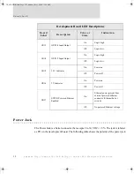
Basic Description

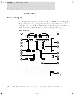
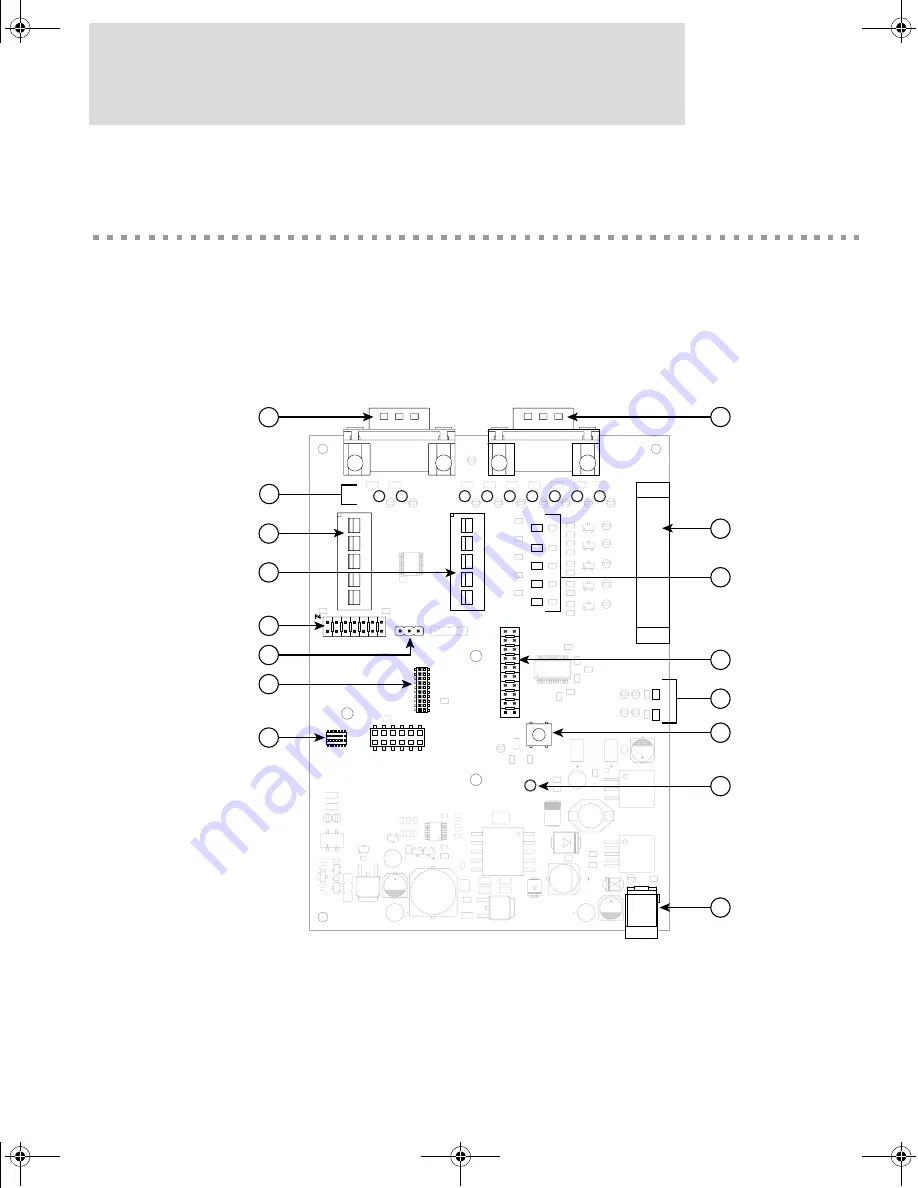
The development board contains connectors, switches, and LEDs for use while integrating 

the embedded module into your design. See the following figure for the location of the 

connectors, switches, and LEDs. Additionally, the board provides test points (not shown on 

the figure). For more information about test points, see "Test points" on page 33. 

Board Layout

00000005

P8

P8

P11

P11

P4

CR2

CR2

P3

P3

CR16

CR16

CR6

CR6

CR15

CR15

P6

P6

SW2

SW2

P9

P9

SW3

SW3

CR4

CR4

CR9

CR9

CR5

CR5

CR1

CR1

P7

P7

P2

P2

SW1

SW1

P1

P1

CR8

CR8

CR7

CR7

CR11

CR11

CR10

CR10

CR13

CR13

CR12

CR12

CR14

CR14

CR3

CR3

CR17

CR17

1

2

3

4

5

6

7

8

10

11

12

13

14

15

16

P12

P12

9

DC_ME-HWR.book  Page 18  Thursday, July 1, 2004  11:12 AM

Summary of Contents for Digi Conntect ME

Page 1: ...TM TM 90000631_A DC_ME HWR book Page 1 Thursday July 1 2004 11 12 AM...

Page 2: ...DC_ME HWR book Page 2 Thursday July 1 2004 11 12 AM...

Page 3: ...not represent a commitment on the part of Digi International Digi provides this document as is without warranty of any kind either expressed or implied including but not limited to the implied warran...

Page 4: ...DC_ME HWR book Page 4 Thursday July 1 2004 11 12 AM...

Page 5: ...wer and Device Interface 12 Connectors Ethernet Interface 13 Connectors Antenna 15 Module LEDs 15 Chapter 2 About the Development Board 17 Overview 17 Basic Description 18 Port Descriptions 20 Connect...

Page 6: ...chanical 45 Dimensions 46 Recommended PCB Layout 51 Antenna Information 53 RF Exposure Statement 54 Safety Statements 55 Appendix B Certifications 57 FCC Part 15 Class B 57 Industry Canada 58 Declarat...

Page 7: ...which are described below About the Integration Kit The integration kit is the ideal platform for product evaluation rapid prototyping and integration of the embedded modules Targeted specifically at...

Page 8: ...ts the specific requirements of your application Related Documentation See the NS7520 Hardware Reference for information on the NS7520 chip Support Information To get help with a question or technical...

Page 9: ...t support or wireless interface From medical systems to building control and industrial automation in virtually any application where embedded device connectivity over Ethernet or wireless connectivit...

Page 10: ...odule with a JTAG interface Note JTAG is a commonly used term that is also referred to as IEEE 1149 1 an industry standard test protocol JTAG is an abbreviation for the European Joint Test Action Grou...

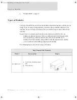
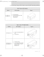
Page 11: ...se in your implementation Digi Connect ME Modules Model Description Figure Digi Connect Wi ME Modules Model Description Figure DC WIME 01T JT Used for development purposes only JTAG interface DC WIME...

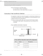
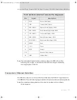
Page 12: ...orts a serial interface with data rates up to 230 400 bps and full modem control and GPIO ports See the following figure for pin orientation and the table for pin assignments Note Digi recommends 100...

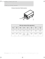
Page 13: ...ure and table for pin orientation and pin assignments Note Pin orientation and assignments are the same for modules with or without a JTAG connector 7 RXD Receive Data Input 8 TXD Transmit Data Output...

Page 14: ...ernet Interface Pin Orientation Ethernet Interface Pin Assignments Pin 1 Pin 2 Pin 3 Pin 4 Pin 5 Pin 6 Pin 7 Pin 8 TXD TXD RXD EPWR EPWR RXD EPWR EPWR Transmit Data Transmit Data Receive Data Power fr...

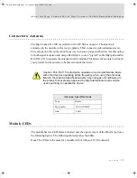
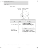
Page 15: ...ide your product but the antenna to be placed outside the device Module LEDs The module has two LEDs that are located near the upper corners of the Ethernet port see the following figure The following...

Page 16: ...rk Link is operational On continuously indicates that an Ethernet connection is made or an access point is engaged Network Activity Diagnostic right upper Green Network Activity On when network traffi...

Page 17: ...ter provides information on development board components and contains the topics listed below For more detailed information on the development board see the schematic and mechanical drawings on the CD...

Page 18: ...ation of the connectors switches and LEDs Additionally the board provides test points not shown on the figure For more information about test points see Test points on page 33 Board Layout 00000005 P8...

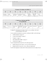
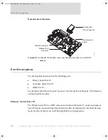
Page 19: ...ion kit Module with JTAG connector for use with a development kit See the following figures for placement of either module onto the development board Connectors Switches and LEDs 1 8 Pin 1 Pin 2 Pin 3...

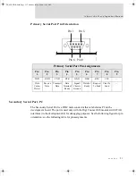
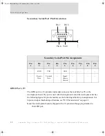
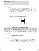
Page 20: ...O Port P3 See the figure titled Board Layout on page 18 for the location of the ports The following sections describe the ports Primary Serial Port P1 The Primary Serial Port is a DB 9 male connector...

Page 21: ...aces in the development kit for debugging purposes See the following figure for pin orientation see the following table for pin assignments Primary Serial Port Pin Assignments Pin 1 Pin 2 Pin 3 Pin 4...

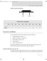
Page 22: ...he development kit See the following figure for pin orientation see the following tables for pin assignments For input and output threshold specifications see DC Characteristics on page 43 Note The de...

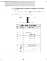
Page 23: ...age 18 for the location of the connectors and blocks The following sections describe the connectors and blocks Embedded Module Connector P7 The Digi Connect ME embedded module Connector is a 20 pin fe...

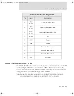
Page 24: ...he figure titled Board Layout on page 18 Embedded Module Connector Pin Orientation Module Connector Pin Assignments Pin Signal Description 1 VETH Power Pass Thru Unused on Digi Connect Wi ME 2 VETH Po...

Page 25: ...e JTAG Debugger Connector P4 Note Because there is no direct connection to the Module JTAG Interface Connector pin orientation and pin assignments are not described for the connector 11 CTS GPIO 2 Cle...

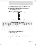
Page 26: ...orientation as shown in the figure titled Board Layout on page 18 JTAG Debugger Connector Pin Orientation Jumper Block P12 This jumper block is reserved for future use Logic Analyzer Header P6 The Lo...

Page 27: ...board provides the following switches GPIO Switch Bank 1 SW1 GPIO Switch Bank 2 SW2 Reset SW3 See the figure titled Board Layout on page 18 for the location of the switches The following sections des...

Page 28: ...communicate with a device The switch is used with the Digi Connect ME embedded module Integration Kit and the Digi Connect ME embedded module Development Kit In addition the switch is used in conjunc...

Page 29: ...can be used independently Notes 1 These switches do not determine whether the GPIO is an input or output That is determined by the module software 2 If GPIO is set to an output by software switch SW2...

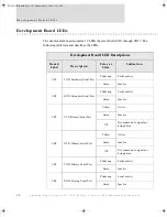
Page 30: ...Indication CR1 TXD Secondary Serial Port Flickering Serial activity Green Inactive CR2 RXD Secondary Serial Port Flickering Serial activity Green Inactive CR3 CTS Primary Serial Port Yellow Active Gr...

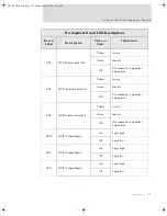
Page 31: ...d or signal not being driven CR9 DSR Primary Serial Port Yellow Active Green Inactive Off Not connected or signal not being driven CR10 GPIO 1 Input Output On Logic high Off Logic low CR11 GPIO 2 Inpu...

Page 32: ...ck CR13 GPIO 4 Input Output On Logic high Off Logic low CR14 GPIO 5 Input Output On Logic high Off Logic low CR15 3 3V Indicator On Power on Off Power off CR16 5V Indicator On Power on Off Power off C...

Page 33: ...e board labels are adjacent to each test point on the board The test point numbers are in the development board schematic drawings The following table lists the test point number board label and a bri...

Page 34: ...Primary Serial Port TP8 RTS RTS Primary Serial Port TP9 DCD DCD Primary Serial Port TP10 DSR DSR Primary Serial Port TP11 GPIO1 GPIO 1 TP12 GPIO2 GPIO 2 TP13 GPIO3 GPIO 3 TP14 GPIO4 GPIO 4 TP15 GPIO5...

Page 35: ...information programmers may require to make use of some Digi Connect ME hardware resources It provides information on the following topics GPIO on page 36 LEDs on page 38 Reset on page 38 Flash on pa...

Page 36: ...pletely describe its behavior and each register is responsible for eight GPIO pins The four bits that describe the GPIO behavior are its mode CMODE its direction CDIR its special function CSF only app...

Page 37: ...DSR GPIO3 PORTA2 Allocated Pin 12 on 20 pin header Used for the serial DSR signal It could be reassigned as either GPIO input or output and used for a general purpose If used in conjunction with the...

Page 38: ...For more information regarding the control of LEDs see the Net Works with GNU Tools BSP Porting Guide About Digi Connect ME LEDs Reset Hard Reset The embedded module supports a hardware reset via pin...

Page 39: ...is exposed via pin 20 on the 20 pin header so it can be controlled by an embedded host When plugged into the development board the INIT signal is pulled high unless a jumper is placed across pins 2 an...

Page 40: ...has 4 MB of flash memory In both modules the flash memory is controlled by chip select 0 located at 0x02000000 Memory The embedded modules have 8 MB of SDRAM memory controlled by chip select 1 locate...

Page 41: ...f duplex and full duplex support auto sensing Connector RJ 45 Standard IEEE 802 11b Frequency 2 4 GHz Data Rate Up to 11 Mbps with automatic fallback Modulation CCK 11 5 Mbps DQPSK 2 Mbps DBPSK 1 Mbps...

Page 42: ...control signals DTR DSR DCD RTS CTS Data Rates bps 50 110 134 150 200 300 600 1200 2400 3600 4800 9600 19200 38400 57600 115200 230400 Flow Control Options RTS CTS XON XOFF None GPIO Five GPIO General...

Page 43: ...gnostic error Operating Conditions Symbol Description Min Typ Max Unit VCC Supply Voltage 3 14 3 3 3 45 V ICC Supply Current Digi Connec t EM 27 0 mA Digi Connec t Wi EM 40 0 IIL Input Current as 0 57...

Page 44: ...n active state When power rises above 2 88V the reset remains for approximately 250 ms to allow the system clock and other circuits to stabilize Environmental Outputs Symbol Description Min Typ Max Un...

Page 45: ...445 in 36 703 mm 1 945 in 49 4 mm Width 0 75 in 19 05 mm Height 0 735 in 18 669 mm Device serial interface connector 20 pin micro header 10 pin double row with 50 inch 1 27 mm pitch Samtec P N FTS 110...

Page 46: ...i g i C o n n e c t M E H a r d w a r e R e f e r e n c e Dimensions The following figures show the dimensions of Digi Connect Wi ME and Digi Connect ME embedded modules Digi Connect Wi ME Module Fro...

Page 47: ...47 M o d u l e S p e c i f i c a t i o n s Bottom DC_ME HWR book Page 47 Thursday July 1 2004 11 12 AM...

Page 48: ...D i m e n s i o n s 4 8 D i g i C o n n e c t W i M E D i g i C o n n e c t M E H a r d w a r e R e f e r e n c e Side DC_ME HWR book Page 48 Thursday July 1 2004 11 12 AM...

Page 49: ...49 M o d u l e S p e c i f i c a t i o n s Digi Connect ME Module Front View DC_ME HWR book Page 49 Thursday July 1 2004 11 12 AM...

Page 50: ...D i m e n s i o n s 5 0 D i g i C o n n e c t W i M E D i g i C o n n e c t M E H a r d w a r e R e f e r e n c e Bottom DC_ME HWR book Page 50 Thursday July 1 2004 11 12 AM...

Page 51: ...ollowing figure shows the recommended PCB printed circuit board layout of the Digi Connect Wi ME and Digi Connect ME It is strongly recommended that you consider using the Digi Connect Wi ME footprint...

Page 52: ...e n d e d P C B L a y o u t 5 2 D i g i C o n n e c t W i M E D i g i C o n n e c t M E H a r d w a r e R e f e r e n c e Digi Connect Wi ME Digi Connect ME DC_ME HWR book Page 52 Thursday July 1 200...

Page 53: ...plane The diagram shows the magnetic field when the antenna is in a vertical position The outside line represents the horizontal plane and the inside dotted line represents the vertical plane Radiati...

Page 54: ...mpt from RF evaluation based on its operating frequency of 2400 MHz and effective radiated power of 100 milliwatts This would be less than the 3 watt requirement for a mobile device 20 cm separation o...

Page 55: ...at least 6 feet from bare power wiring or lightning rods and associated wires and at least 6 inches from other wire antenna wires doorbell wires wires from transformers to neon signs steam or hot wat...

Page 56: ...Electrical Code Article 800 Contact a licensed electrician for details DC_ME HWR book Page 56 Thursday July 1 2004 11 12 AM Modular Device End User Responsibility If the FCC ID is not visible when ins...

Page 57: ...ith the instruction manual may cause harmful interference to radio communications However there is no guarantee that interference will not occur in a particular installation If this equipment does cau...

Page 58: ...s or modifications to this equipment not expressly approved by Digi may void the user s authority to operate this equipment Industry Canada This digital apparatus does not exceed the Class B limits fo...

Page 59: ...e product listed above has been tested at an External Test Laboratory certified per FCC rules and has been found to meet the FCC Part 15 Class B Emission Limits Documentation is on file and available...

Page 60: ...ed modules meet the following electromagnetic emissions standards EN55022 EN55024 EN 300 324 EN 301 489 VCCI AS 3548 RSS 210 Digi Connect Wi ME IC 1846A 50M880 FCC Part 15 Subpart C Digi Connect Wi ME...

Page 61: ...ample Application TTL Signals to EIA 232 A P P E N D I X C The following schematic is an example of how to convert the modules s TTL signals to EIA 232 DC_ME HWR book Page 61 Thursday July 1 2004 11 1...

Page 62: ...8 7 6 5 4 3 2 1 DB9 P1 RS 232 SERIAL 9 PIN CONNECTOR SHIELD SHIELD GND GND 17 13 25 24 16 15 14 12 28 21 1 20 3 6 2 7 19 18 22 23 26 27 5 4 8 9 ADM211E U1 RS 232 LINE RECVR 5RX 4TX 5V GND 12 11 10 9...

Page 63: ...DC_ME HWR book Page 63 Thursday July 1 2004 11 12 AM...

Page 64: ...DC_ME HWR book Page 64 Thursday July 1 2004 11 12 AM...

Reviews: