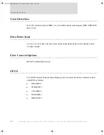

E n v i r o n m e n t a l
4 4
D i g i C o n n e c t W i - M E & D i g i C o n n e c t M E H a r d w a r e R e f e r e n c e
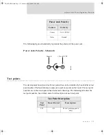
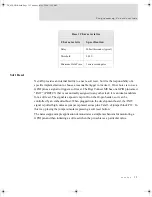
Note
The embedded modules provide an on board supervisor circuit with a 2.88V
reset threshold and an internal 5k pull-up resistor. When VCC falls to the
threshold voltage, a reset pulse is issued, holding the output in active state.
When power rises above 2.88V, the reset remains for approximately 250 ms to
allow the system clock and other circuits to stabilize.
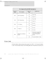
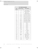
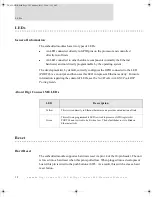
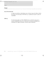
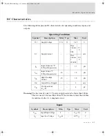
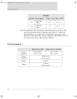
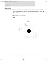
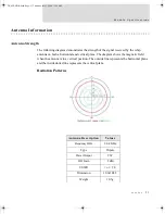
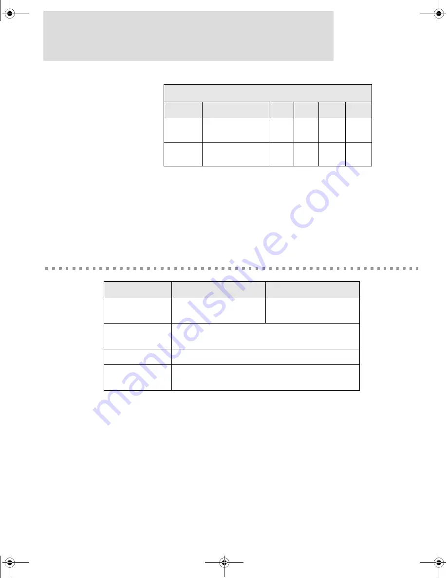
Environmental
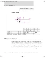
Outputs
Symbol
Description
Min
Typ
Max
Unit
V
OH
Output High
Voltage
2.4
—
3.45
V
V
OL
Output Low
Voltage
0
—
0.4
V
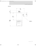
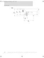
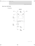
Digi Connect ME
Digi Connect Wi-ME
Ambient
Temperature
-40
o
F to 185
o
F
(-40
o
C to 85
o
C)
-4
o
F to 185
o
F
(-20
o
C to 85
o
C)
Storage
Temperature
-40
0
F to 257
0
F
(-40
0
C to 125
0
C)
Humidty
5% to 90%
Altitude
12000 feet
(3657.60 meters)
DC_ME-HWR.book Page 44 Thursday, July 1, 2004 11:12 AM
Summary of Contents for Digi Conntect ME
Page 1: ...TM TM 90000631_A DC_ME HWR book Page 1 Thursday July 1 2004 11 12 AM...
Page 2: ...DC_ME HWR book Page 2 Thursday July 1 2004 11 12 AM...
Page 4: ...DC_ME HWR book Page 4 Thursday July 1 2004 11 12 AM...
Page 63: ...DC_ME HWR book Page 63 Thursday July 1 2004 11 12 AM...
Page 64: ...DC_ME HWR book Page 64 Thursday July 1 2004 11 12 AM...


