Hardware
Design notes
XBee 868LP RF Modules User Guide
24
Do not connect any pins that are not in use. Use the
PR
and
PD
commands to pull all inputs on the
radio high or low with 40k internal pull-up or pull-down resistors. Unused outputs do not require any
specific treatment.
For applications that need to ensure the lowest sleep current, never leave unconnected inputs
floating. Use internal or external pull-up or pull-down resistors, or set the unused I/O lines to outputs.
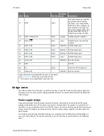
You can connect other pins to external circuitry for convenience of operation including the Associate
LED pad (pad 28) and the Commissioning pad (pad 33). The Associate LED pad flashes differently
depending on the state of the module to the network, and a pushbutton attached to pad 33 can
enable various join functions without having to send serial port commands. For more information see
Commissioning pushbutton and associate LED
. The source and sink capabilities are limited to 6 mA on
all I/O pads.
Only the programmable versions of these devices use the VREF pad (pad 27). For compatibility with
other XBee modules, we recommend connecting this pin to a voltage reference if you want to enable
analog sampling. Otherwise, connect to GND.
Design notes for PCB antenna devices
Position PCB antenna devices so there are no ground planes or metal objects above or below the
antenna. For best results, do not place the device in a metal enclosure, as this may greatly reduce the
range. Place the device at the edge of the PCB on which it is mounted. Make sure the ground, power
and signal planes are vacant immediately below the antenna section.
The following drawings illustrate important recommendations when you are designing with PCB
antenna devices. For optimal performance, do not mount the device on the RF pad footprint described
in the next section, because the footprint requires a ground plane within the PCB antenna keep out
area.


